
Second-order band-pass filter and wireless apparatus using the same

a filter and second-order technology, applied in waveguides, basic electric elements, waveguide type devices, etc., can solve the problems of not meeting the requirements of wlan devices for out-band rejection, occupying too much space in the rf circuit, and difficult to realize in a standard motherboard

Active Publication Date: 2010-10-26
MEDIATEK INC
View PDF6 Cites 3 Cited by
  • Summary
  • Abstract
  • Description
  • Claims
  • Application Information

AI Technical Summary

Benefits of technology

The present invention provides a second-order band-pass filter and a wireless apparatus using the same. The filter includes a first and second transmission line resonator, an impedance inverter, and a plurality of bending. The filter has one end open-circuit towards a first direction and the other end open-circuit towards a second direction. The impedance inverter is coupled between the first and second transmission line resonators, and includes an inductor, microstrip lines, and another inductor. The wireless apparatus includes a transceiver and the second-order band-pass filter. The filter is used for filtering radio signals received or transmitted by the transceiver. The technical effect of the invention is to provide a high-quality filter with improved performance and stability for wireless applications.

Problems solved by technology

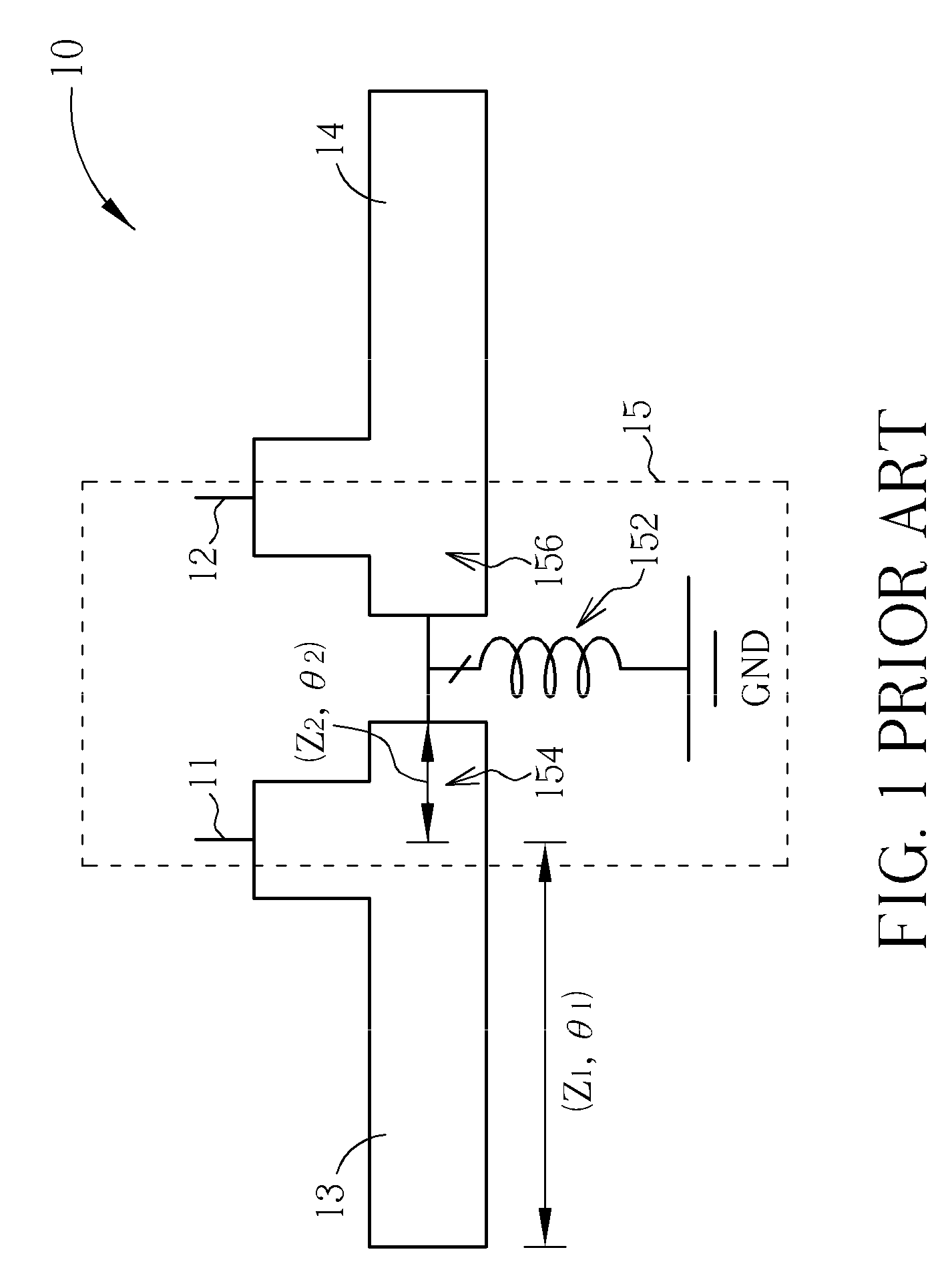
However, at present, such design is seldom applied to a front-end circuit of a Wireless Local Area Network (WLAN) device, especially those operated near an ISM (Industrial, Scientific and Medical) band of the United States, mainly because a high-order microwave band-pass filter is needed to achieve a sufficient Out-Band Rejection capability.
Even though the high-order microwave band-pass filter has a steep cut-off frequency response characteristic, due to its large overall length or size, it often occupies too much space in the RF circuit.
Thus, it is hard to realize in a standard motherboard, and is contrary to the design demands of the modern communications device, which emphasizes lightness, thinness, smallness, etc.
However, for such second-order band-pass filters, the frequency response in a lower frequency part of the pass-band is still similar to that of a common second-order band-pass filter, which cannot satisfy out-band rejection requirements of the WLAN devices.

Method used


Image

  • Second-order band-pass filter and wireless apparatus using the same
  • Second-order band-pass filter and wireless apparatus using the same
  • Second-order band-pass filter and wireless apparatus using the same

Examples


Embodiment Construction

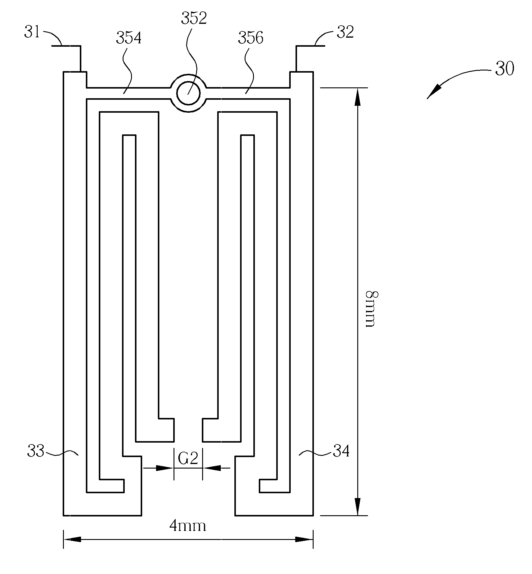
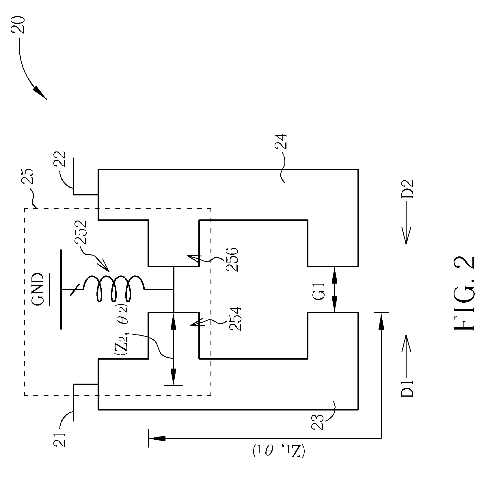
[0016]Please refer to FIG. 2. FIG. 2 is a schematic diagram of a second-order band-pass filter 20 utilized for a wireless apparatus according to the present invention. The second-order band-pass filter 20 is utilized for generating at least two transmission zeros, and includes a first signal terminal 21, a second signal terminal 22, a first transmission line resonator 23, a second transmission line resonator 24 and an impedance inverter 25. The first signal terminal 21 and the second signal terminal 22 are for the use of signal input and output. The first transmission line resonator 23 is formed by bending a quarter-wavelength open stub, and has one end coupled to the first signal terminal 21 and the other end open-circuited in a first direction D1. The second transmission line resonator 24 is symmetric to the first transmission line resonator 23 and formed by bending a quarter-wavelength open stub as well, and has one end coupled to the second signal terminal 22 and the other end o...


PUM


Abstract

A second-order band-pass filter for generating at least two transmission zeros includes a first signal terminal, a second signal terminal, a first transmission line resonator, a second transmission line resonator and an impedance inverter. The first transmission line resonator and the second transmission line resonator are symmetric to each other and coupled to the first signal terminal and the second signal terminal, which are formed by bending two quarter-wavelength open stubs and have an open circuit gap between the two terminals. The impedance inverter includes an inductor, a first micro strip line and a second micro strip line. The first micro strip line and the second micro strip line are symmetric to each other, and are coupled to the first signal terminal and the second signal terminal and coupled to a ground through the inductor, respectively.

Description

BACKGROUND OF THE INVENTION[0001]1. Field of the Invention[0002]The present invention relates to a second-order band-pass filter and a wireless apparatus using the same, and more particularly, to a second-order band-pass filter and a wireless apparatus using the same that bends two quarter-wavelength open stubs to form a cross coupling structure for generating at least two transmission zeros.[0003]2. Description of the Prior Art[0004]In a RF front-end circuit of a modern communications device, a band-pass filter is an important and essential component for reducing unnecessary emission of harmonics and parasitic signals from a transmitter, or enhancing noise elimination capability of a receiver when receiving signals. Generally, an operation frequency of the modern communications device is substantially located at a microwave band, and thus it is an economical and practical approach to realize the band-pass filter on a printed circuit board (PCB) in the form of a transmission line, w...

Claims


Application Information

Patent Timeline
Patent Type & Authority Patents(United States)
IPC IPC(8): H01P1/203
CPCH01P1/20327
Inventor HSU, MIN-SHUN
Owner MEDIATEK INC
Learn More