
High performance flash memory devices (FMD)

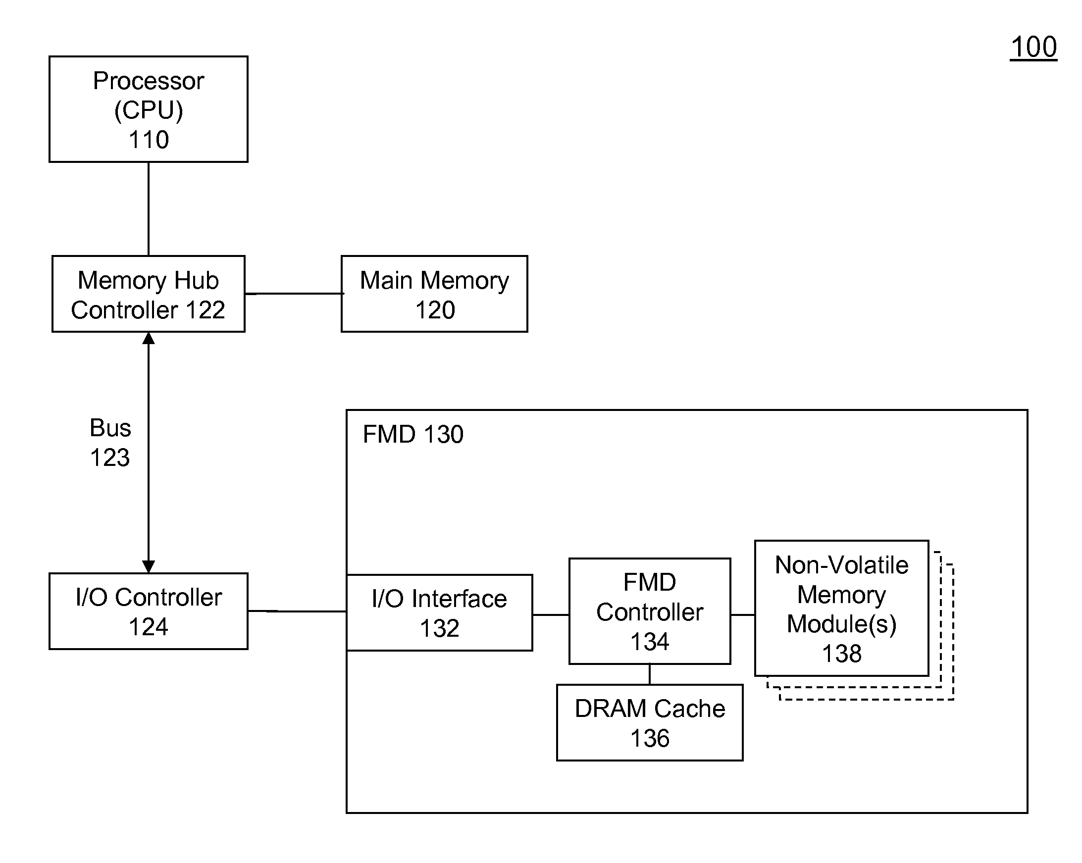
a flash memory, high-performance technology, applied in the field of flash memory devices, can solve the problems that non-volatile memory based secondary storage cannot achieve high performance, and achieve the effect of high performance, high-performance data transfer, and no sacrificing performan

Inactive Publication Date: 2010-11-02
SUPER TALENT TECH CORP
View PDF9 Cites 80 Cited by
  • Summary
  • Abstract
  • Description
  • Claims
  • Application Information

AI Technical Summary

Benefits of technology

[0011]According to yet another aspect, data transfers between the set of data buffers and the at least one non-volatile memory chips are conducted through all of the data channels in parallel, thereby achieving high performance. To further increase efficiency and performance, data transfer to and from each of the vertical groups may also be conducted in parallel.

Problems solved by technology

However, the non-volatile memory based secondary storage has not been able to achieve high performance, such as the level of the performance defined in Ultra Direct Memory Access (UDMA).

Method used


Image

  • High performance flash memory devices (FMD)
  • High performance flash memory devices (FMD)
  • High performance flash memory devices (FMD)

Examples


Embodiment Construction

[0042]In the following description, numerous specific details are set forth in order to provide a thorough understanding of the present invention. However, it will become obvious to those skilled in the art that the present invention may be practiced without these specific details. The descriptions and representations herein are the common means used by those experienced or skilled in the art to most effectively convey the substance of their work to others skilled in the art. In other instances, well-known methods, procedures, components, and circuitry have not been described in detail to avoid unnecessarily obscuring aspects of the present invention.

[0043]Reference herein to “one embodiment” or “an embodiment” means that a particular feature, structure, or characteristic described in connection with the embodiment can be included in at least one embodiment of the invention. The appearances of the phrase “in one embodiment” in various places in the specification are not necessarily ...


PUM


Abstract

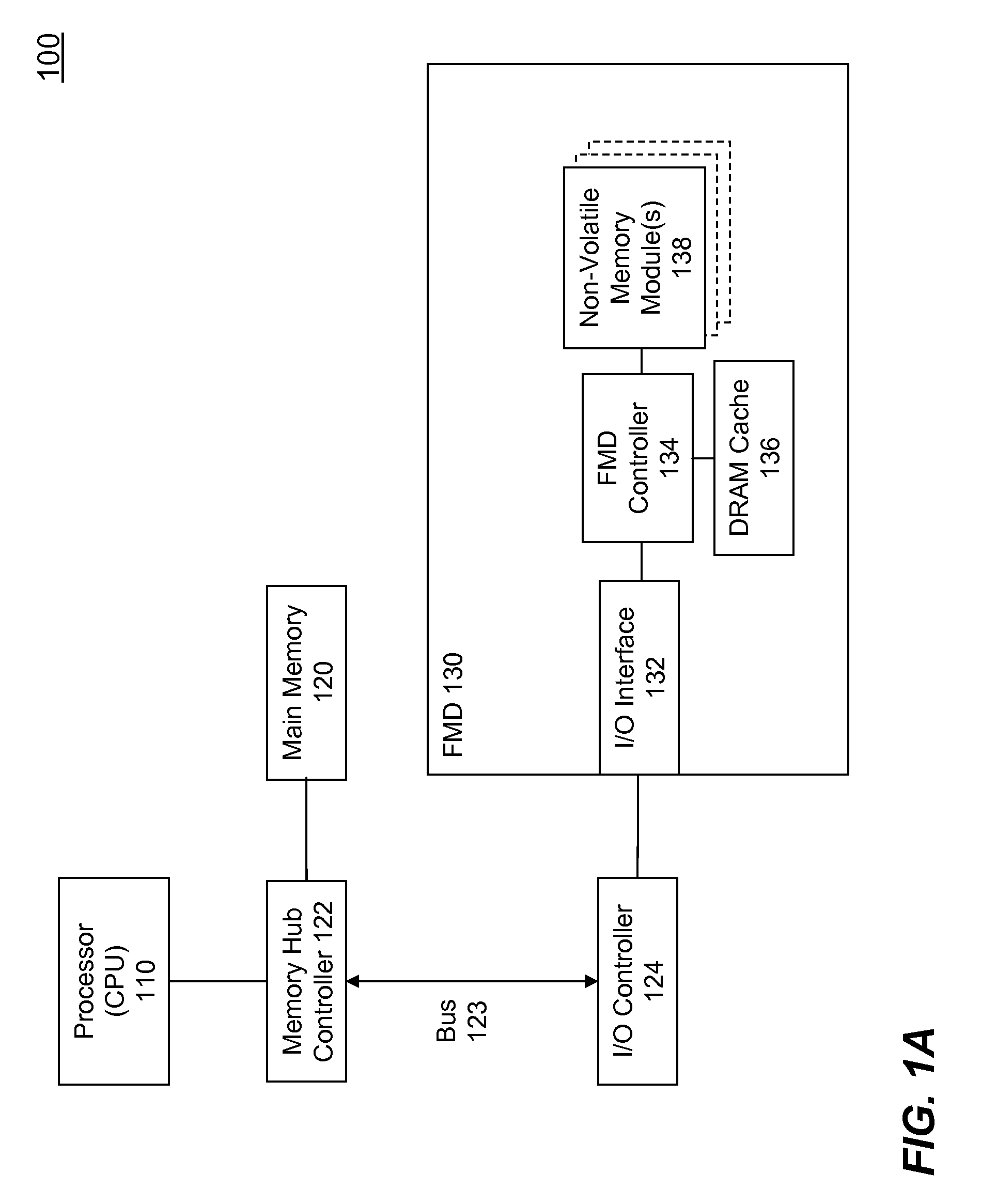
High performance flash memory devices (FMD) are described. According to one exemplary embodiment of the invention, a high performance FMD includes an I / O interface, a FMD controller, and at least one non-volatile memory module along with corresponding at least one channel controller. The I / O interface is configured to connect the high performance FMD to a host computing device The FMD contoller is configured to control data transfer (e.g., data reading, data writing / programming, and data erasing) operations between the host computing device and the non-volatile memory module. The at least one non-volatile memory module, comprising one or more non-volatile memory chips, is configured as a secondary storage for the host computing device. The at least one channel controller is configured to ensure proper and efficient data transfer between a set of data buffers located in the FMD controller and the at least one non-volatile memory module.

Description

CROSS-REFERENCE TO RELATED APPLICATIONS[0001]This application is a continuation-in-part (CIP) of U.S. patent application for “Local Bank Write Buffers for Acceleration a Phase Change Memory”, U.S. application Ser. No. 11 / 748,595, filed May 15, 2007, now U.S. Pat. No. 7,471,556, which is CIP of “Flash Memory System with a High Speed Flash Controller”, application Ser. No. 10 / 818,653, filed Apr. 5, 2004, now U.S. Pat. No. 7,243,185, content of which is incorporated herein as though set forth in full.FIELD OF THE INVENTION[0002]The present invention relates to flash memory devices used in computer systems, and more particularly to methods and systems for providing high performance flash memory device (FMD) in computer systems.BACKGROUND OF THE INVENTION[0003]Personal computers have become mainstream computing devices for the past two decades. One of the core components of a personal computer whether desktop or laptop is a mother board, which is the central or primary circuit board prov...

Claims


Application Information

Patent Timeline
Patent Type & Authority Patents(United States)
IPC IPC(8): G06F12/00
CPCG06F11/1068G11C5/04
Inventor LEE, CHARLES C.YU, I-KANGCHOW, DAVID Q.MA, ABRAHAM CHIH-KANGSHEN, MING-SHIANG
Owner SUPER TALENT TECH CORP
Learn More