Method for manufacturing semiconductor device

a semiconductor and manufacturing method technology, applied in semiconductor/solid-state device testing/measurement, instruments, printing, etc., can solve the problems of high processing accuracy, difficult to understand circuit structure or wiring arrangement, and difficult to design complex integrated circuits, so as to achieve the effect of increasing the kinds of materials which can be used for manufacturing semiconductor devices and efficient use of materials

Inactive Publication Date: 2010-11-02
SEMICON ENERGY LAB CO LTD
View PDF12 Cites 1 Cited by
  • Summary
  • Abstract
  • Description
  • Claims
  • Application Information

AI Technical Summary

Benefits of technology

[0013]If the diameter d of the droplet landed is determined, a width of a line which can be obtained is almost determined as well. Accordingly, limitation of narrowness of the width of the line which can be obtained with the ink-jet apparatus largely depends on the head. If a minute wiring or the like is desired to be formed with the ink-jet apparatus in manufacturing of an electric circuit, a head with which a line width of the minute wiring can be obtained needs to be prepared. As a nozzle diameter of the head is smaller and more delicate, higher processing accuracy is needed, which makes the head expensive. Further, when a plurality of lines are desired to be obtained at close intervals with the ink-jet apparatus, the droplet discharged from the head of the ink-jet apparatus spreads on the surface to be processed after landing; therefore, it is difficult to form a plurality of lines in a high density in a certain area.
[0018]Thus, a wiring of which width is narrower than the diameter of the droplet landed can be formed and a conventional etching step can be omitted. Further, since an ink-jet method is used, a material can be used efficiently. Conventionally, a metal film is formed over the entire surface of the substrate, and then the metal film is selectively removed by wet etching or dry etching using a photolithography technique to form a wiring; therefore, loss of a material is large and a process thereof is complex. Further, depending on etching conditions, there is a possibility that etching is performed to a material layer in addition to the metal film which is desired to be etched.
[0019]For mass production, it is greatly advantageous to omit a conventional etching step. An etching apparatus is not required, and influence of etching to another layer does not need to be worried. The kinds of materials which can be used for manufacturing the semiconductor device can be increased.
[0021]Further, the present invention is devised in making the raster data. The raster data with which discharging is performed to all coordinate squares corresponding to a pattern to be obtained is not made. In the present invention, the number of discharging droplets is reduced in accordance with a basic pattern and the number of basic patterns in series to determine the most suitable number of discharging droplets. When a plurality of lyophilic regions of which widths are narrower than the diameter of the droplet are arranged, one droplet can be divided and a plurality of wirings can be obtained efficiently. For example, a thin wiring is not placed so that a distance between a thick wiring and the thin wiring is more than the diameter of the droplet landed. The distance between the thick wiring and the thin wiring is set closer than the diameter of the droplet landed, whereby the wirings can be obtained efficiently.

Problems solved by technology

When a complex integrated circuit is formed, it is difficult to understand a circuit structure or a wiring arrangement, only from this raster data and this raster bitmap.
Further, it is also difficult to design the complex integrated circuit only by using the raster data or the raster bitmap from the beginning.
As a nozzle diameter of the head is smaller and more delicate, higher processing accuracy is needed, which makes the head expensive.
Further, when a plurality of lines are desired to be obtained at close intervals with the ink-jet apparatus, the droplet discharged from the head of the ink-jet apparatus spreads on the surface to be processed after landing; therefore, it is difficult to form a plurality of lines in a high density in a certain area.

Method used


Image

  • Method for manufacturing semiconductor device
  • Method for manufacturing semiconductor device
  • Method for manufacturing semiconductor device

Examples


embodiment mode 1

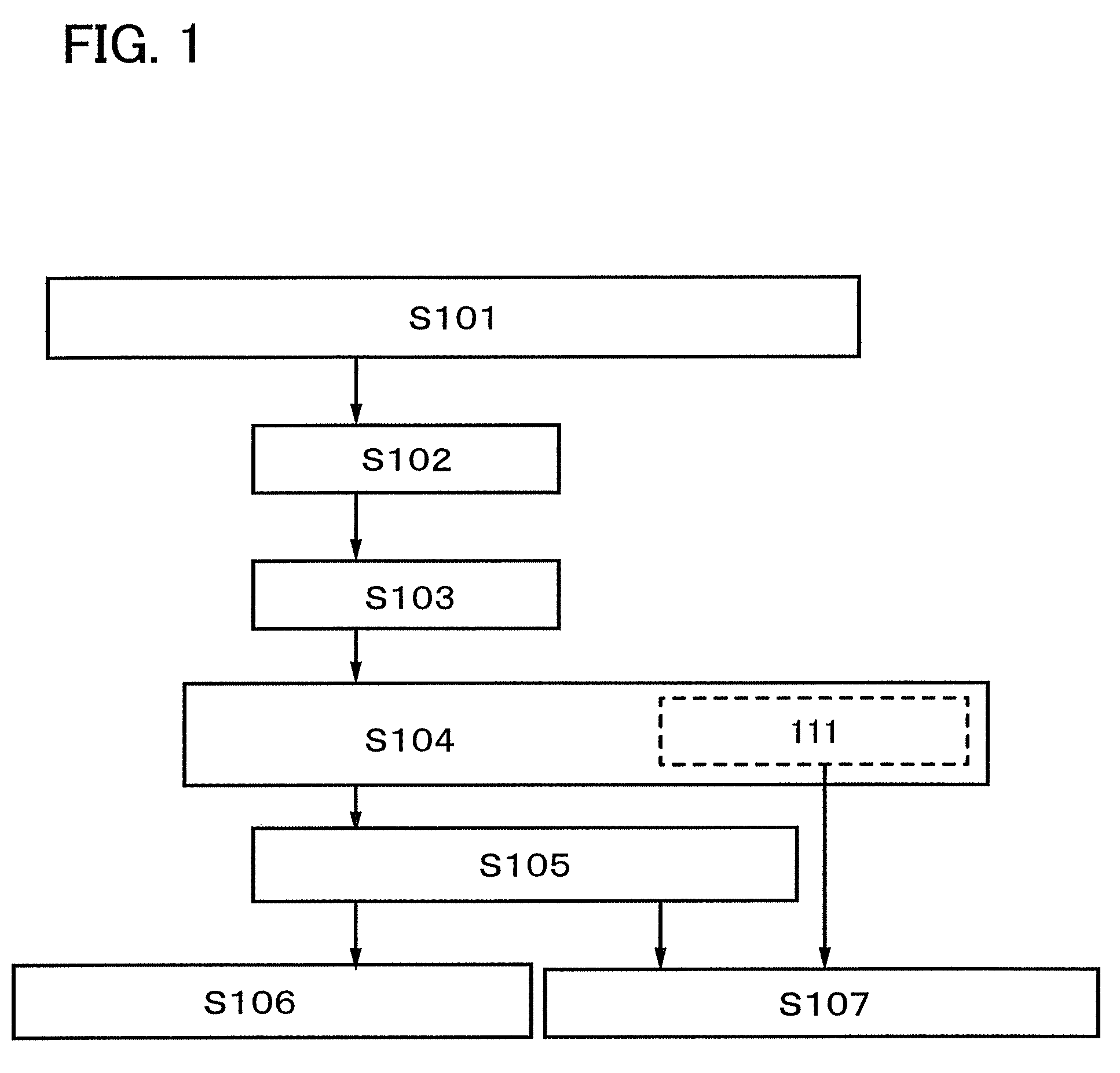
[0052]In this embodiment mode, procedures of manufacturing a mask and making raster data will be explained with reference to FIG. 1.

[0053]First, a droplet is discharged over a surface to be processed by a droplet discharging apparatus, and measurement of a diameter d of the droplet landed is performed (S101). By measurement of the diameter d of the droplet, a design unit of the mask and the raster data is determined.

[0054]Next, coordinates are made regarding a size of greater than or equal to 50% and less than 90% of the diameter d of the droplet as one unit (S102). Here, this one unit is referred to as a dot pitch, and each block of the coordinates is a square element having a dot pitch dpx (a main scanning direction)×a dot pitch dpy (a sub scanning direction). However, one element of the coordinates is not limited to a square and may have a rectangle where dpx≠dpy.

[0055]Next, a circuit is designed in order to determine arrangement or the like of a wiring to be obtained using a dro...

embodiment mode 2

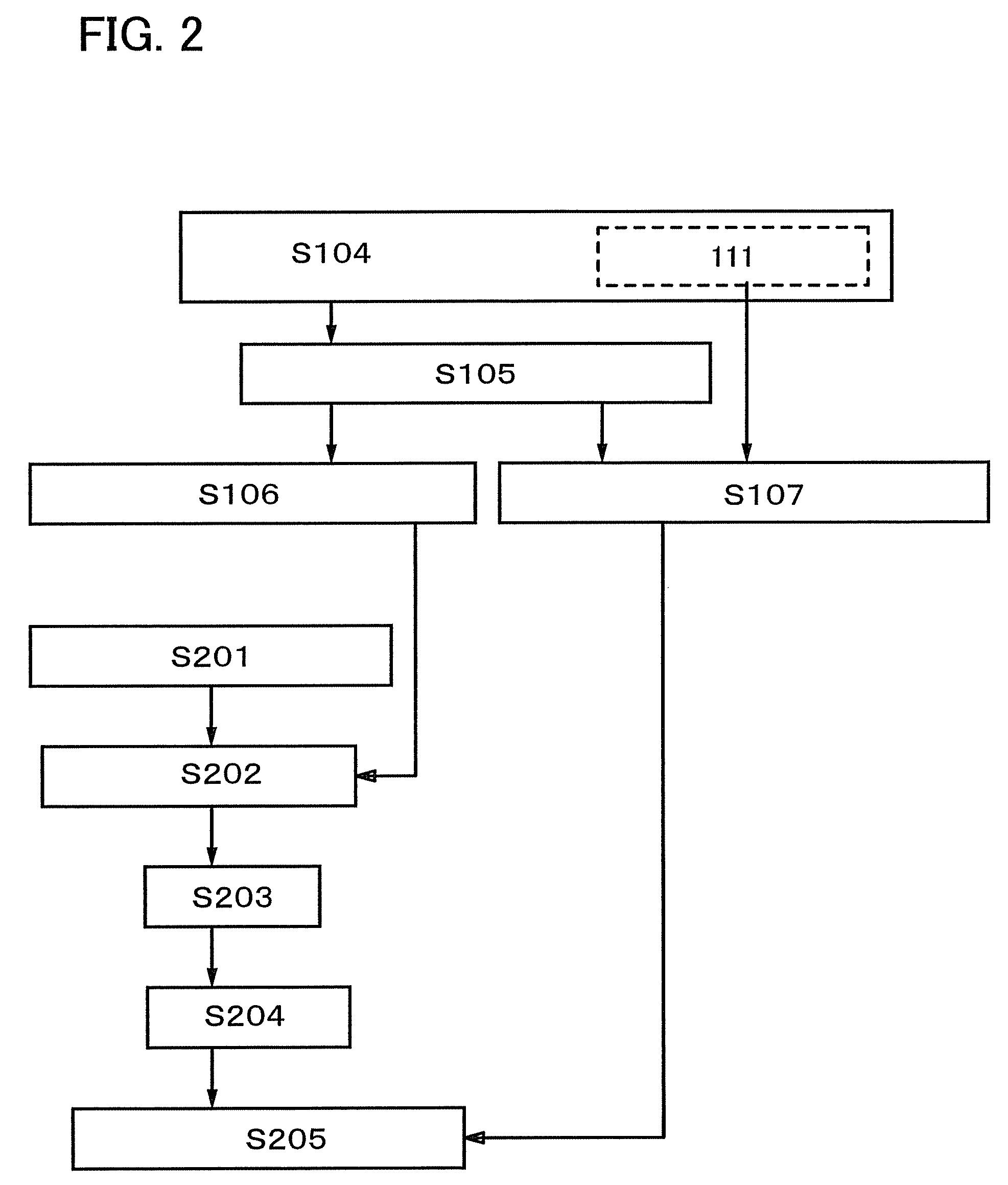
[0063]Here, flow until a droplet of a conductive material is discharged over a surface to be processed will be explained with reference to FIG. 2. Note that the same reference numerals are used for parts which are in common with FIG. 1. A method for forming a wiring mainly containing silver by discharging a droplet including silver nanoparticle over the surface to be processed of a glass substrate will be explained hereinafter.

[0064]First, a resist is applied over the surface to be processed (S201). As a resist material, a positive type resist or a negative type resist is used. Here, a glass substrate of which surface to be processed is formed of an inorganic material is used. In order to improve adhesiveness with the silver nanoparticle, the negative type resist is used.

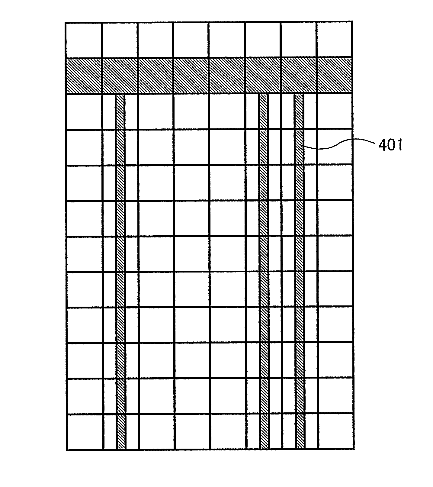
[0065]Next, light exposure is performed using the mask formed in Embodiment Mode 1 as a light-exposure mask (S202). FIG. 4A shows an example of a layout of the mask. The light-exposure mask is a light shielding mask...

embodiment mode 3

[0076]Here, examples of a mask design diagram and examples of raster data in which block patterns different from those shown in FIG. 4 are used will be described with reference to FIG. 5A to FIG. 6B.

[0077]FIG. 5A is a mask design diagram which is made using three kinds of block patterns B1, C1, D1 selected from the diagram registering library.

[0078]FIG. 5A is the mask design diagram when a source wiring and a drain electrode of a thin film transistor are formed with the ink-jet apparatus. A light shielding mask which has openings in places shown by shaded portions 501 in FIG. 5A is made.

[0079]FIG. 5B shows an example of the raster data corresponding to FIG. 5A. Discharging is performed the same number of times (20) as the number of patterns to the places corresponding to the block pattern D1. Discharging is performed once for three continuous pitches to the places corresponding to the block pattern C1. Further, the most suitable pitches in the Y direction, that is, in the scanning d...


PUM


Abstract

When a design diagram of the semiconductor device by a conventional CAD tool is used, a pattern which can be formed with the ink-jet apparatus is limited; therefore, there is a possibility that some circuits of the desired semiconductor device cannot be formed as they are designed. A plurality of basic patterns which can be obtained by discharging with the ink-jet apparatus are prepared, and layout of a desired integrated circuit is performed by combining the patterns. A light-exposure mask is formed based on the layout obtained. Light exposure is performed using the light-exposure mask. Then, development is performed, and the resist film remains in the light-exposed region of which width is narrower than the diameter of the droplet landed. Liquid repellent treatment is performed to an exposed portion on the surface, and then the material droplet is dropped over the resist film. Discharging is selectively performed by a droplet discharging method to form a wiring of which width is narrower than the dot diameter.

Description

BACKGROUND OF THE INVENTION[0001]1. Field of the Invention[0002]The present invention relates to a semiconductor device having a circuit which includes a thin film transistor (hereinafter referred to as a TFT), and a manufacturing method thereof. For example, the present invention relates to an electronic appliance in which an electro-optical device typified by a liquid crystal display panel or a light-emitting display device having an organic light-emitting element is mounted as a part thereof.[0003]Applicants claim priority under 35 U.S.C. §119 to the following foreign application: Serial no. 2006-351985 filed Dec. 27, 2006 in Japan.[0004]In this specification, the semiconductor device refers to all devices that can function by using semiconductor characteristics, and an electro-optical device, a semiconductor circuit, and an electronic appliance are all included in the semiconductor device.[0005]2. Description of the Related Art[0006]In recent years, attention has been focused on...

Claims


Application Information

Patent Timeline
Patent Type & Authority Patents(United States)
IPC IPC(8): G06F17/50
CPCH01L22/12H01L2924/0002H01L2924/00B41J2/01G02F1/13
Inventor FUJII, GENTAKAHASHI, ERIKA
Owner SEMICON ENERGY LAB CO LTD
Why Eureka
Try Eureka