Narrow spectrum light source

a narrow spectrum light source and wavelength spectrum technology, applied in the field of integrated optics and vcsels, can solve the problems of relatively high signal attenuation of waveguides and not suitable for most applications

Active Publication Date: 2010-11-16
OCTROLIX
View PDF5 Cites 136 Cited by
  • Summary
  • Abstract
  • Description
  • Claims
  • Application Information

AI Technical Summary

Benefits of technology

[0028]The present invention provides a narrow-spectrum light source that avoids some of the costs and disadvantages of the prior art.
[0033]Using this preferred material system enables a narrow-spectrum light source that is far simpler in terms of components and layout than the prior art. In the illustrative embodiment, the narrow-spectrum light source simply comprises a VCSEL and a ring resonator that are optically coupled to one another by waveguides. In the illustrative embodiment, the ring resonator and the waveguides that optically couple the ring resonator to the VCSEL are implemented using the preferred material system. In some embodiments, the narrow spectrum light source is implemented on a single chip. In some embodiments, the narrow spectrum light source is monolithically integrated. The result is a narrow spectrum light source, which can be VCSEL based, that is substantially easier to manufacture and is less costly than the arrangement disclosed in U.S. Pat. No. 6,690,687. And all of these benefits accrue from the use of the preferred material system.
[0039](1) the loop waveguide should be formed via a high-contrast waveguide technology so that it can have a small size and thus a large free spectral range;
[0042]The preferred material system is high contrast, yet it enables efficient coupling. This is accomplished by including a large amount of nitride, but in the form of substantially thinner layers than other material systems. Therefore, using the preferred material system, the loop waveguide and the port waveguides can be formed in the same material system. In addition to resolving the apparent conflict, this reduces fabrication costs.
[0044]The preferred material system comprises materials that can be deposited via LPCVD. Most surface waveguides are formed using materials that are not compatible with LPCVD and instead require PECVD. LPCVD is preferred over PECVD because it enables large batch processing, whereas PECVD requires small batch processing (e.g., one or two wafers at a time). Large batch processing can enable significant production cost reductions.
[0045]In addition to narrowing the spectral bandwidth of the VCSEL, the ability to the tune the resonant wavelength of the ring resonator (e.g., thermo-optically, electro-optically, etc.) provides an ability to affect small changes to the nominal center wavelength of the VCSEL. This is accomplished by setting the resonant frequency of the ring resonator such that it is not equal to the nominal center frequency of the VCSEL. It is notable that the integrated Bragg gratings of the VCSEL will serve to prevent re-entry into the VCSEL of “off-resonance” light. As a consequence, if an ability to alter the nominal center wavelength of the VCSEL is desired, the external “mirror” (i.e., ring resonator) must have a smaller bandwidth than the VCSEL's integrated Bragg grating.

Problems solved by technology

Unfortunately, high contrast waveguides generally have relatively high signal attenuation; therefore, they are not suitable for most applications.

Method used


Image

  • Narrow spectrum light source
  • Narrow spectrum light source
  • Narrow spectrum light source

Examples


Embodiment Construction

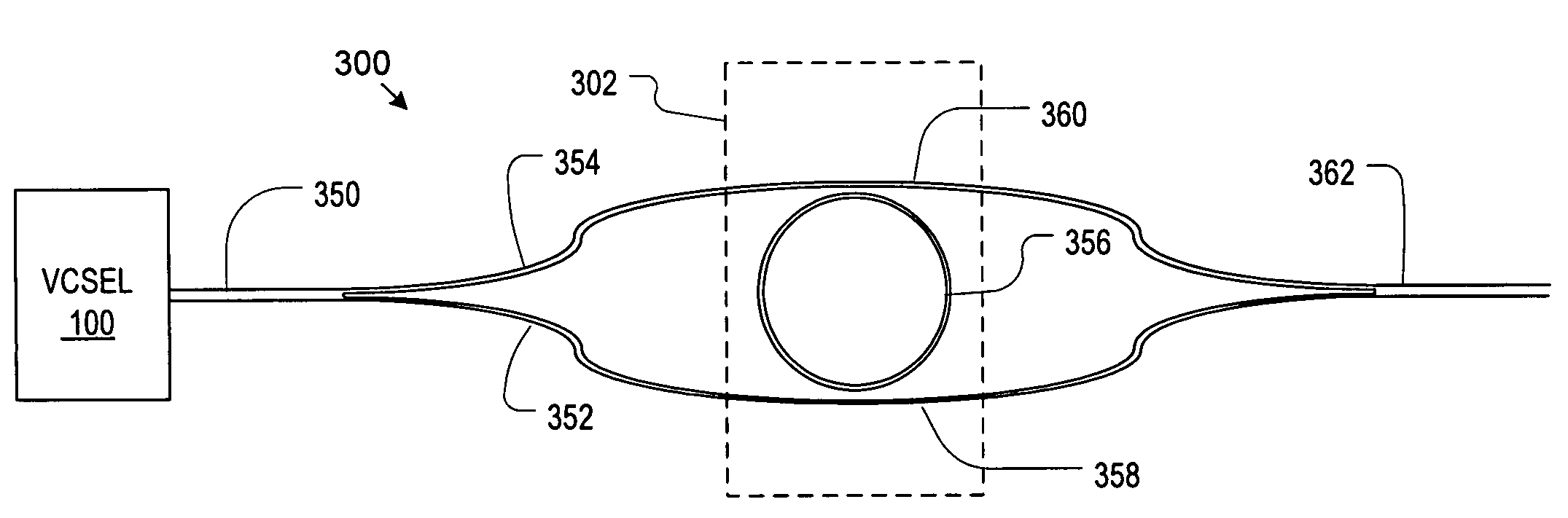
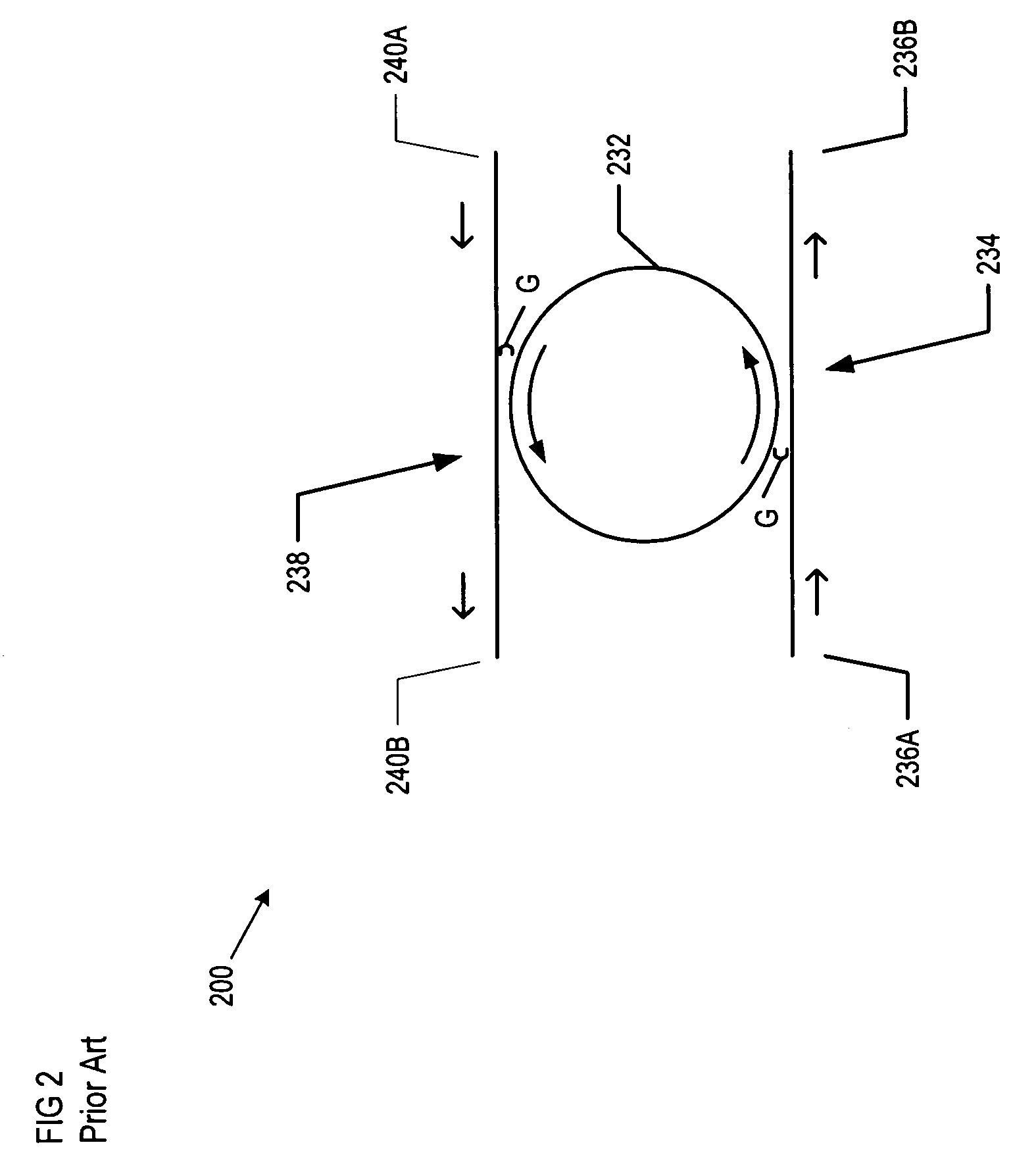
[0053]The terms that appear below are provided with the following explicit definitions for use in understanding the specification and interpreting the appended claims:[0054]Free spectral range is the distance (in frequency or wavelength space) between adjacent transmission peaks.[0055]Spectral component refers to optical energy characterized by a particular wavelength, such as is typically present in the emission from a laser. In the context of real-world technological applications, as opposed to a theoretical discussion, a spectral component will never actually be characterized by only a single wavelength. Rather, the electromagnetic spectrum of the spectral component will include a plurality of wavelengths that are centered about a predominant, primary or center wavelength.[0056]Evanescent-coupling relation refers to a relationship between two or more elements, typically optical waveguides, wherein an optical signal traveling through one of the elements is capable of coupling at l...


PUM


Abstract

An apparatus and method are disclosed for decreasing the spectral bandwidth of a semiconductor laser, such as a vertical cavity surface emitting laser.

Description

FIELD OF THE INVENTION[0001]The present invention relates to integrated optics and VCSELs.BACKGROUND OF THE INVENTION[0002]Lasers are ubiquitous; they are used for many different purposes and in a variety of applications. One type of semiconductor laser that has recently garnered much attention is the vertical cavity surface emitting laser, commonly known by the acronym “VCSEL.”[0003]Semiconductor diode-lasers comprise a plurality of layers of semiconductor material that is sandwiched between two “mirrors.” Photon generation occurs principally in an optical gain region, where charge carriers (i.e., electrons and holes) from n- and p-doped regions of the device combine and emit energy as photons. The mirrors force most of these emitted photons to return through the gain region. As they do, the photons stimulate the recombination of other charge carriers, which in-turn generates more photons. These newly generated photons are characterized by the same wavelength as the photons that st...

Claims


Application Information

Patent Timeline
Patent Type & Authority Patents(United States)
IPC IPC(8): H01S3/083H01S5/00G02B6/42H01S3/10
CPCH01S5/065H01S5/0612H01S5/0654H01S5/0656H01S5/1021H01S5/1071H01S5/142H01S5/18358H01S3/083
Inventor HEIDEMAN, RENE GERRITKLEIN, EDWIN JAN
Owner OCTROLIX
Why Eureka
Try Eureka