Organic light emitting device including photo responsive material and a method of fabricating the same

a technology of organic light-emitting devices and photoresponsive materials, which is applied in the direction of organic semiconductor devices, discharge tubes/lamp details, nuclear engineering, etc., can solve the problems of unsuitable solution process and difficult formation of large-sized organic active layers having a uniform thickness, and achieve the effect of simplifying the overall fabrication process

Active Publication Date: 2010-11-23
SAMSUNG ELECTRONICS CO LTD
View PDF5 Cites 21 Cited by
  • Summary
  • Abstract
  • Description
  • Claims
  • Application Information

AI Technical Summary

Benefits of technology

[0008]The present invention provides an organic light emitting device (OLED) with a high-efficiency, long-lifespan organic active layer, and a method of fabricating the OLED, in which the overall fabrication process is simplified by using a solution process and the molecular arrangement structure in an organic active layer gradually varies according to depth, so that a mobility gradient of the mobility of holes and electrons varies gradually.
[0009]According to an aspect of the present invention, there is provided a method of fabricating an organic light emitting device, the method including forming a lower substrate on a substrate; depositing an organic active material solution containing at least one photoreactive material on the lower substrate to form an organic active material layer, and radiating light onto the organic active material layer so that a characteristic of the light varies according to the depth of the organic active material layer in order to gradually vary a molecular orientation structure in the organic active material layer according to the depths, thereby resulting in a carrier mobility gradient according to the depths of the organic active material layer.

Problems solved by technology

However, it is difficult to form a large-sized organic active layer having a uniform thickness by the conventional vapor deposition process.
However, fundamentally this solution process is not suitable for forming a multi-layer structure because a solvent used to form an upper layer may melt a lower layer.

Method used


Image

  • Organic light emitting device including photo responsive material and a method of fabricating the same
  • Organic light emitting device including photo responsive material and a method of fabricating the same
  • Organic light emitting device including photo responsive material and a method of fabricating the same

Examples


Embodiment Construction

[0037]Embodiments of the present invention will be described with reference to the appended drawings.

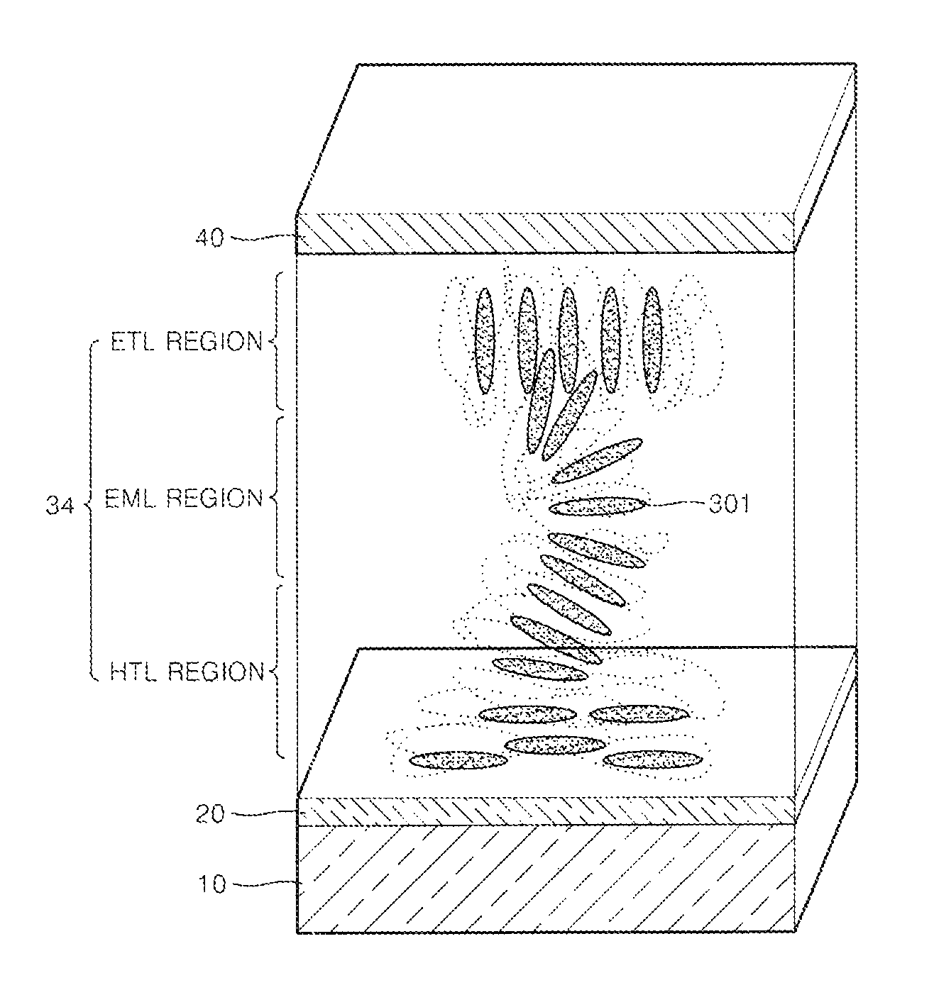
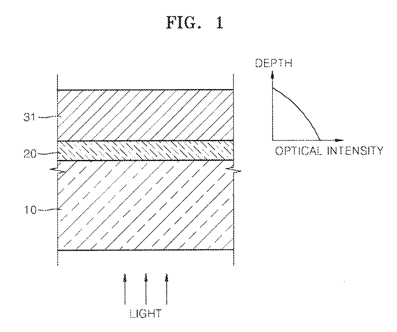
[0038]FIG. 1 is a view for illustrating a method of varying or differentiating the intensity of light absorbed by an organic active layer according to depth. Initially, an electrode 20 is formed on a substrate 10. Here, the substrate 10 may be one of a glass substrate or a transparent plastic substrate, but the present invention is not limited thereto. The substrate may also be a planar structure in which different functional structures are formed. For example, when manufacturing an active matrix type OLED display panel, a substrate may include an organic thin film transistor (OTFT) structure. The electrode 20 may be any conductive material thin film which can function as an anode or a cathode depending on the applied voltage. In the current embodiment, the substrate 10 and the electrode 20, both of which are optically transparent, and the electrode 20 functioning as an anode are des...


PUM

PropertyMeasurementUnit
thicknessaaaaaaaaaa
thicknessaaaaaaaaaa
carrier mobilityaaaaaaaaaa

Abstract

Provided is a method of fabricating an organic light emitting device using a solution process. The method includes forming an electrode on a lower substrate; depositing an organic active material solution containing at least one photoreactive material on the electrode to form an organic active material layer; and radiating light onto the organic active material layer so that a characteristic of the light varies according to the depth of the organic active material layer in order to gradually vary a molecular orientation structure in the organic active material layer according to the depths, thereby resulting in a carrier mobility gradient according to the depths of the organic active material layer.

Description

CROSS-REFERENCE TO RELATED PATENT APPLICATIONS[0001]This application claims the benefit of Korean Patent Application No. 10-2007-0089956, tiled on Sep. 5, 2007, in the Korean Intellectual Property Office, the disclosure of which is incorporated herein in its entirety by reference.BACKGROUND OF THE INVENTION[0002]1. Field of the Invention[0003]The present invention relates to an organic light emitting device (OLED) and a method of fabricating the same and more particularly, to an OLED having an organic active layer with a new molecular orientation structure and a method of fabricating the OLED in which the organic active layer is formed using a solution process.[0004]2. Description of the Related Art[0005]Organic light emitting devices (OLED), which include an anode, a cathode, and an organic active layer including a fluorescent or phosphorescent organic compound between the anode and the cathode, are self-emissive devices which spontaneously emit light as holes supplied from the ano...

Claims


Application Information

Patent Timeline
Patent Type & Authority Patents(United States)
IPC IPC(8): H01L51/00H01L51/56
CPCH01L51/5012H05B33/10H01L51/5048H01L51/0039H01L51/0076H01L51/5052H01L51/56H01L2251/5346H10K85/115H10K85/731H10K50/14H10K50/155H10K50/165H10K50/11H10K2101/80H10K71/00H05B33/14
Inventor KIM, HEE-KYUNGAHN, PIL-SOO
Owner SAMSUNG ELECTRONICS CO LTD
Why Eureka
Try Eureka