Multi-path accessible semiconductor memory device having mailbox areas and mailbox access control method thereof

a multi-path accessible, mailbox technology, applied in the direction of memory adressing/allocation/relocation, digital storage, instruments, etc., can solve the problems of increasing the configuration cost of memory, reducing the number of message input/output lines performing an input/output of message with the mailbox, and reducing the number of chip input/output lines. , the effect of substantially reducing the number of messages

Inactive Publication Date: 2010-11-23
SAMSUNG ELECTRONICS CO LTD
View PDF25 Cites 95 Cited by
  • Summary
  • Abstract
  • Description
  • Claims
  • Application Information

AI Technical Summary

Benefits of technology

[0026]The present general inventive concept provides a multipath accessible semiconductor memory device having a mailbox area, and a mailbox access control method thereof, in which a message is transmitted through a shared data input / output path or through a specifically adapted common message input / output path. A chip size can be substantially reduced. Further, a number of message input / output lines performing an input / output of message with the mailbox can be substantially reduced.

Problems solved by technology

Thus it is difficult to ensure a satisfactory data transmission speed, causing a complication in the size and increasing expenses for the configuration of memories.
It is therefore difficult to apply the multiprocessor system of FIG. 2 to a typical DRAM because of the structure of memory banks or ports.
Such interfaces cause a limitation in speed, an increase in the number of pins, etc.

Method used


Image

  • Multi-path accessible semiconductor memory device having mailbox areas and mailbox access control method thereof
  • Multi-path accessible semiconductor memory device having mailbox areas and mailbox access control method thereof
  • Multi-path accessible semiconductor memory device having mailbox areas and mailbox access control method thereof

Examples


Embodiment Construction

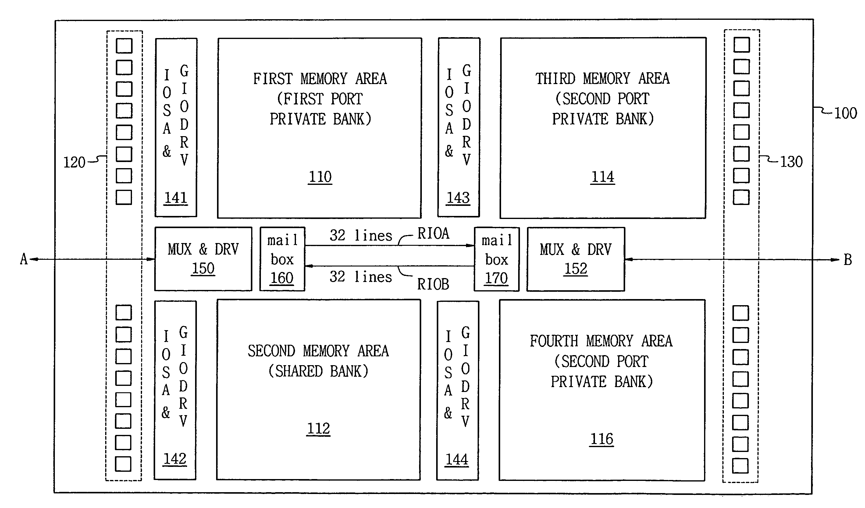
[0057]Reference will now be made in detail to the embodiments of the present general inventive concept, examples of which are illustrated in the accompanying drawings, wherein like reference numerals refer to the like elements throughout. The embodiments are described below in order to explain the present general inventive concept by referring to the figures.

[0058]Unless otherwise defined, all terms (including technical and scientific terms) used herein have the same meaning as commonly understood by one of ordinary skill in the art to which this present general inventive concept belongs. It will be further understood that terms used herein should be interpreted as having a meaning that is consistent with their meaning in the context of this specification and the relevant art and will not be interpreted in an idealized or overly formal sense unless expressly so defined herein. Exemplary embodiments of the present general inventive concept are more fully described below with referenc...


PUM


Abstract

A multipath accessible semiconductor memory device having a mailbox area and a mailbox access control method thereof are provided. The semiconductor memory device includes N number of ports, at least one shared memory area allocated in a memory cell array, and N number of mailbox areas for message communication. The at least one shared memory area is operationally connected to the N number of ports, and is accessible through a plurality of data input / output lines to form a data access path between the at least one shared memory area and one port, having an access right to the at least one memory area, among the N number of ports. The N number of mailbox areas are provided in one-to-one correspondence with the N number of ports and are accessible through the plurality of data input / output lines when an address of a predetermined area of the at least one shared memory area is applied to the semiconductor memory device. An efficient layout of mailboxes and an efficient message access path can be obtained.

Description

CROSS-REFERENCE TO RELATED APPLICATIONS[0001]This application claims priority under 35 U.S.C. §119 from Korean Patent Application 10-2007-0005158, filed on Jan. 17, 2007, the contents of which are hereby incorporated by reference in their entirety for all purposes as if fully set forth herein.BACKGROUND OF THE INVENTION[0002]1. Field of the Invention[0003]The present general inventive concept relates to semiconductor memory devices. More particularly, the present general inventive concept relates to a multipath accessible semiconductor memory device having mailbox areas and a mailbox access control method thereof.[0004]2. Description of the Related Art[0005]In general, a semiconductor memory device having a plurality of access ports is called a multiport memory, and in particular a memory device having two access ports is called a dual-port memory. A typical dual-port memory is well-known in the field, as an image processing video memory having a RAM port accessible in a random sequ...

Claims


Application Information

Patent Timeline
Patent Type & Authority Patents(United States)
IPC IPC(8): G06F12/00
CPCG11C5/02G11C8/12G06F13/16G06F12/00G06F15/167G06F15/16
Inventor OH, CHI-SUNGKIM, YONG-JUNNAM, KYUNG-WOOKIM, JIN-KUKKIM, SOO-YOUNG
Owner SAMSUNG ELECTRONICS CO LTD
Why Eureka
Try Eureka