Structure for on-chip electromigration monitoring system

a monitoring system and electromigration technology, applied in the field of microelectronic structures, can solve the problems of forming a void in the metal, affecting the reliability of the system, so as to reduce the voltage stress level of the chip, improve system performance, and delay the expected failure time of the chip.

Active Publication Date: 2010-11-23
META PLATFORMS INC
View PDF12 Cites 7 Cited by
  • Summary
  • Abstract
  • Description
  • Claims
  • Application Information

AI Technical Summary

Benefits of technology

[0007]Accordingly, in view of the problems mentioned above in relation to the prior art, it would be desirable to provide a design structure embodied in a machine-readable medium used in a design process, the design structure including an on-chip EM sensor which monitors a degradation of a semiconductor chip due to EM during the useful lifetime of the chip, i.e., when the chip is packaged and installed in a system for normal use. When the resistance of a wiring element within the semiconductor chip increases beyond a warning threshold level, either the chip is replaced or a voltage stress level of the chip is reduced in a way that delays the expected failure time of the chip. In such way, customers are permitted to trade increased system performance in exchange for increased lifetime of the chip. In addition, in accordance with the embodiments of the present invention described herein, operators of systems which include a defective chip having over threshold resistance are permitted to replace the defective chip before the defective chip jeopardizes the whole system, thereby preventing the system from crashing unpredictably.
[0008]Therefore, in accordance with an aspect of the invention, a design structure embodied in a machine readable medium used in a design process can include apparatus of a semiconductor chip operable to detect an increase in resistance of a monitored element of the semiconductor chip. The design structure can include, for example, a resistive voltage divider circuit operable to output a plurality of reference voltages having different values. A plurality of comparators in the semiconductor chip may be coupled to receive the reference voltages and a monitored voltage representative of a resistance of the monitored element. Each of the comparators may produce an output indicating whether the monitored voltage exceeds the reference voltages, so that the resistance value of the monitored element may be precisely determined.

Problems solved by technology

Electromigration is indeed one of the worst reliability concerns affecting integrated circuits throughout the last 50 years.
Failure due to electromigration is caused by a positive divergence of the ionic flux leading to an accumulation of vacancies and forming a void in the metal.
EM becomes worse as the width and / or thickness of metal wiring on the chip are scaled.
The approaches described therein poorly reflect the actual EM failure mechanism because neither the dummy feature nor the methodology used to test for electromigration are representative of actual conditions which lead to EM failures of conductive interconnects on the chip.
The dummy feature fails to adequately represent real-life conductive interconnects which have topology including corners and via contact regions.
Accelerated test methodology, while predictive of future failures which might occur during later use of the chip, fails to detect failures at time points during the actual useful lifetime of the chip.
Moreover, the dummy features tested in accordance with such approaches are bulky and are usually provided within a kerf area adjacent to a chip, or inside a specially designed test chip of the wafer.
The above-described prior art approaches do not provide for monitoring the effects of EM throughout the useful lifetime of the chip.
However, it is abundantly evident that EM degradation does not stop after the chip is installed in a system and shipped to customers.

Method used


Image

  • Structure for on-chip electromigration monitoring system
  • Structure for on-chip electromigration monitoring system
  • Structure for on-chip electromigration monitoring system

Examples


Embodiment Construction

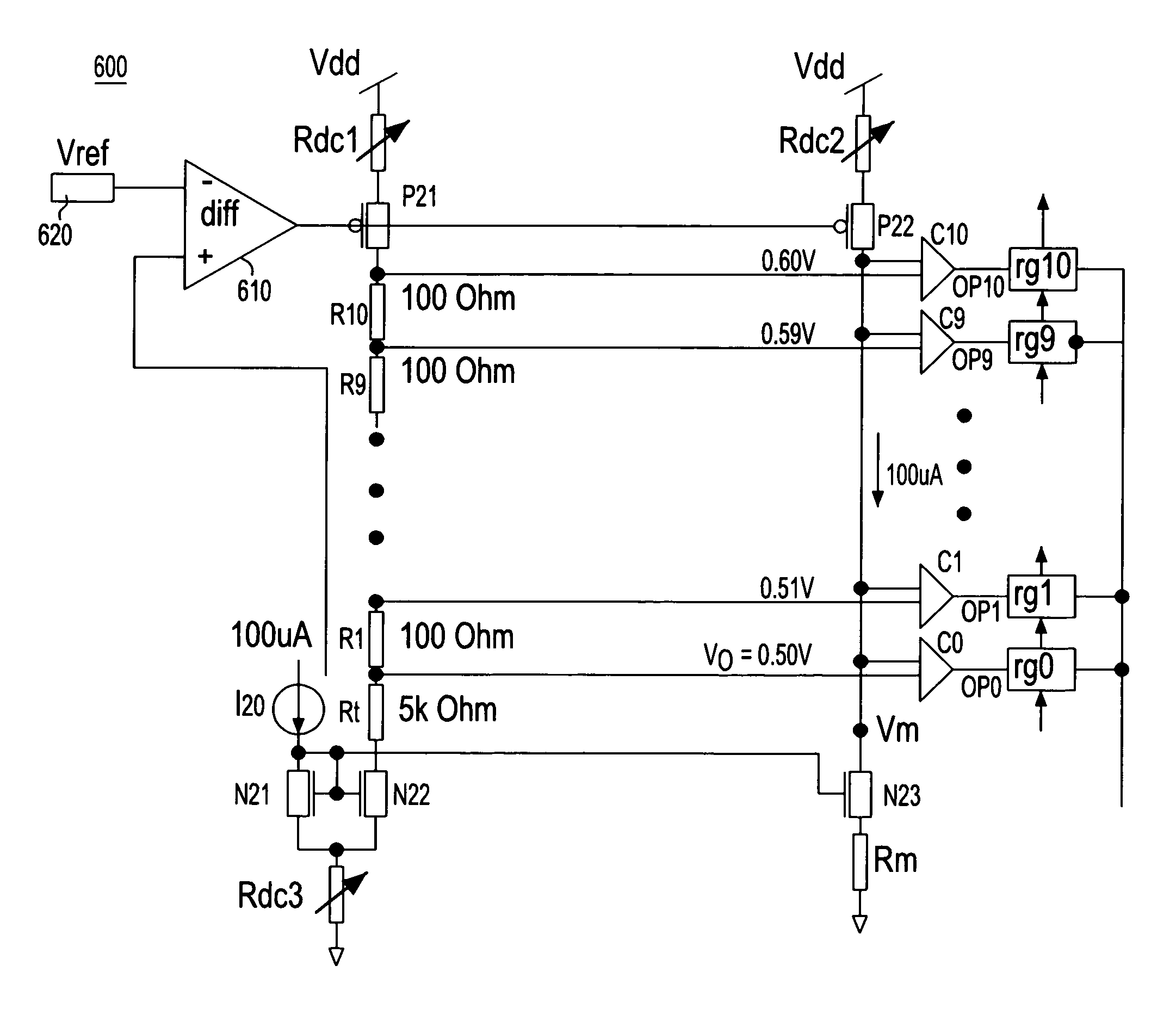
[0019]Commonly owned U.S. patent application Ser. No. 11 / 306,985 filed Jan. 18, 2006 to Louis L. Hsu et al. entitled “On-Chip Electromigration Monitoring System” is incorporated by reference herein.

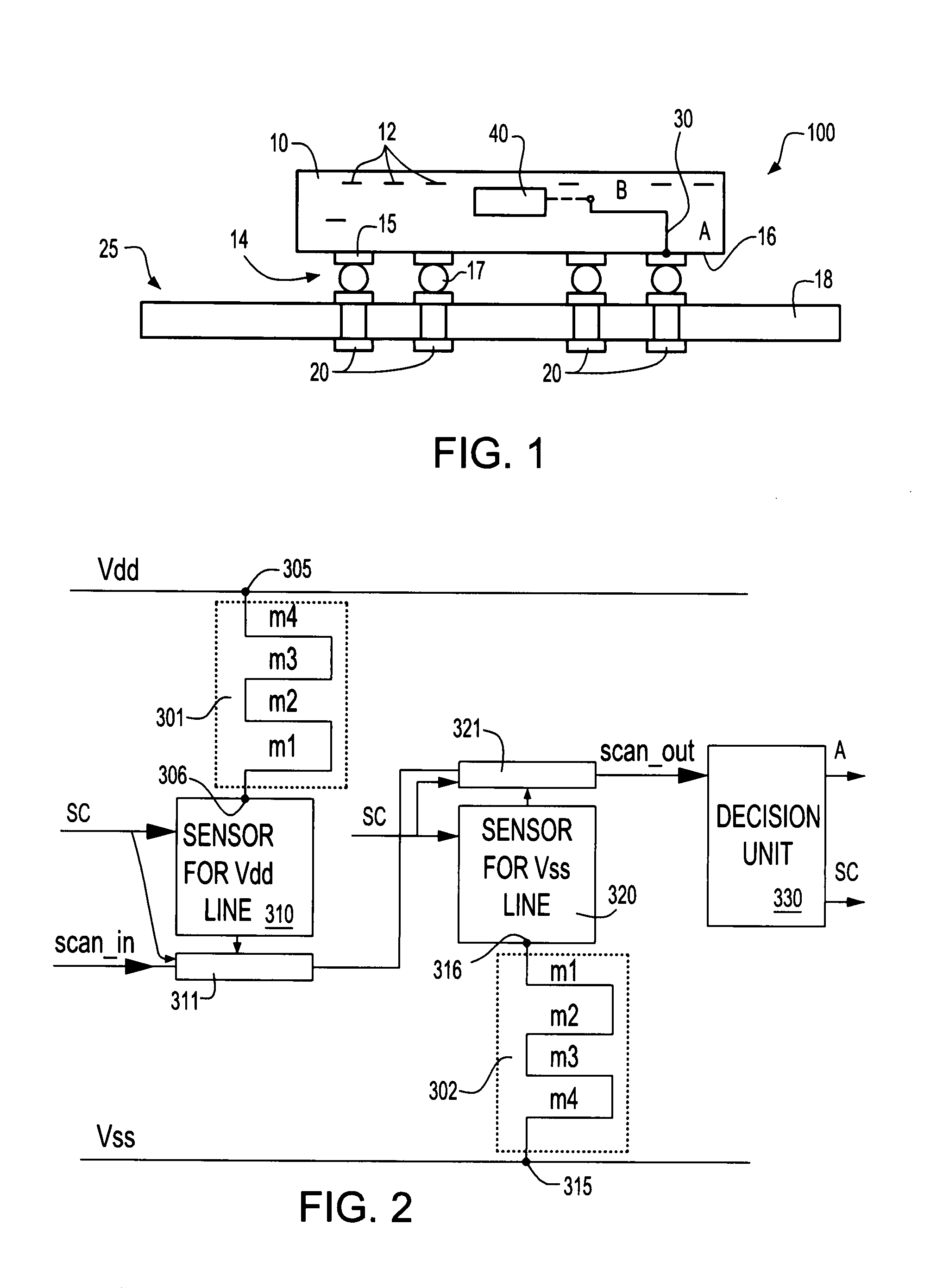
[0020]Referring to FIG. 1, a first embodiment of the invention will now be described. FIG. 1 illustrates a packaged chip 100 such as may be installed and operated in a larger scale electronic system, e.g., a computing and / or communications system, among others. Thus, the apparatus and test method described herein are usable at a time after wafer-level test time. Preferably, they are usable at a time when the packaged chip is installed in such electronic system for normal operation. As such, the packaged chip includes more than a bare semiconductor chip and includes that which is needed to conductively connect the conductive contacts of the semiconductor chip to the package element. An exemplary packaged chip 100 will now be described which includes a semiconductor chip and a package eleme...


PUM


Abstract

A design structure embodied in a machine readable medium used in a design process can include apparatus of a semiconductor chip operable to detect an increase in resistance of a monitored element of the semiconductor chip. The design structure can include, for example, a resistive voltage divider circuit operable to output a plurality of reference voltages having different values. A plurality of comparators in the semiconductor chip may be coupled to receive the reference voltages and a monitored voltage representative of a resistance of the monitored element. Each of the comparators may produce an output indicating whether the monitored voltage exceeds the reference voltages, so that the resistance value of the monitored element may be precisely determined.

Description

BACKGROUND OF THE INVENTION[0001]The present invention relates to microelectronic structures and methods of making them and more particularly to a system provided on a chip for monitoring an increase in a resistance of a conductive interconnect of a chip due to electromigration.[0002]Electromigration has long been identified as a major failure mechanism of metal interconnects of semiconductor chips. Electromigration is indeed one of the worst reliability concerns affecting integrated circuits throughout the last 50 years. Electromigration tends to produce voids within metal conductors) due to movement of metal ions in directions parallel to high density current flow within the chip. Failure due to electromigration is caused by a positive divergence of the ionic flux leading to an accumulation of vacancies and forming a void in the metal. To the casual observer, it appears that ions are moved “downstream” by the force of “electron wind”.[0003]For the reasons stated above, electromigr...

Claims


Application Information

Patent Timeline
Patent Type & Authority Patents(United States)
IPC IPC(8): G06F17/50
CPCG06F17/5036G01R31/2858G06F30/367
Inventor HSU, LOUIS L.CRANFORD, JR., HAYDEN C.GLUSCHENKOV, OLEGMASON, JAMES S.SORNA, MICHAEL A.YANG, CHIH-CHAO
Owner META PLATFORMS INC
Why Eureka
Try Eureka