Light-emitting diode, light-emitting device, lighting apparatus, display, and signal light

a light-emitting device and light-emitting diode technology, applied in semiconductor devices, instruments, electrical devices, etc., can solve the problems of reducing the light emission amount, light emission efficiency, and the use of icp-rie, and achieve the effect of high light emission efficiency and large light emission amoun

Inactive Publication Date: 2010-11-30
NAPRA
View PDF13 Cites 31 Cited by
  • Summary
  • Abstract
  • Description
  • Claims
  • Application Information

AI Technical Summary

Benefits of technology

[0010]It is an object of the present invention to provide a light-emitting diode with a large light emission amount and a hig

Problems solved by technology

As a matter of course, this also decreases the light emission amount, as well as the light emission efficiency.
The ICP-RIE, which is used for many purposes in Si micromachining (MEMS), as well as for high-frequency dev

Method used


Image

  • Light-emitting diode, light-emitting device, lighting apparatus, display, and signal light
  • Light-emitting diode, light-emitting device, lighting apparatus, display, and signal light
  • Light-emitting diode, light-emitting device, lighting apparatus, display, and signal light

Examples


first embodiment

(1) Light-Emitting Device

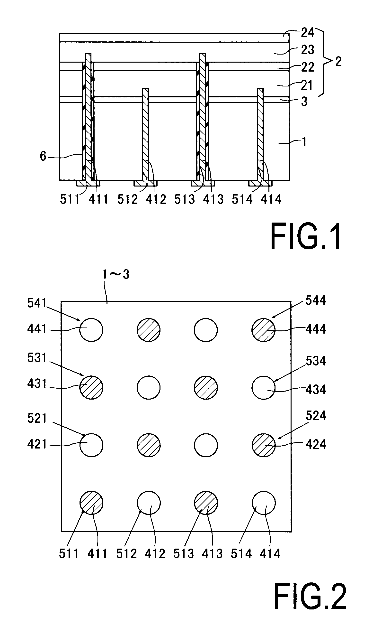
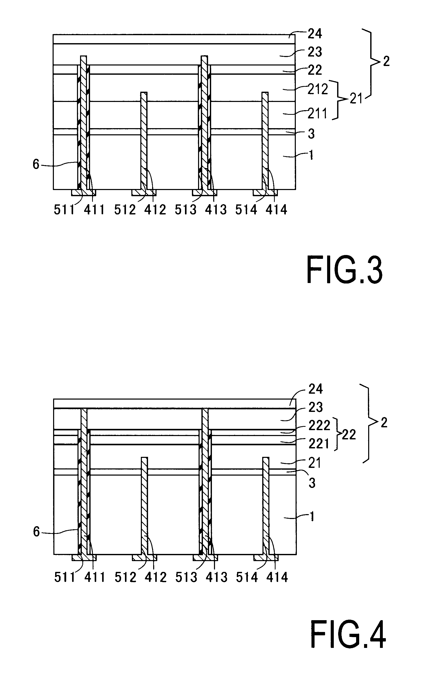
[0068]Referring to FIG. 7, the light-emitting device according to a first embodiment includes a light-emitting diode LED and a phosphor 8. The light-emitting diode LED is the light-emitting diode according to the present invention, which has been described with reference to FIGS. 1 to 4. The phosphor 8 is disposed at the light-emitting side of the light-emitting diode LED for emitting light of a different color from that of the light-emitting diode LED.

[0069]If a blue light-emitting diode is used for the light-emitting diode LED and a substance which emits light whose color is complementary to blue light emitted from the blue light-emitting diode is used for the phosphor 8, for example, there is obtained white light (visible light). If a GaN-based compound semiconductor is used for the blue light-emitting diode, a YAG-based phosphor 8 can be used for the corresponding phosphor 8.

[0070]However, colored light from the light-emitting device, which varies over a...

second embodiment

(2) Light-Emitting Device

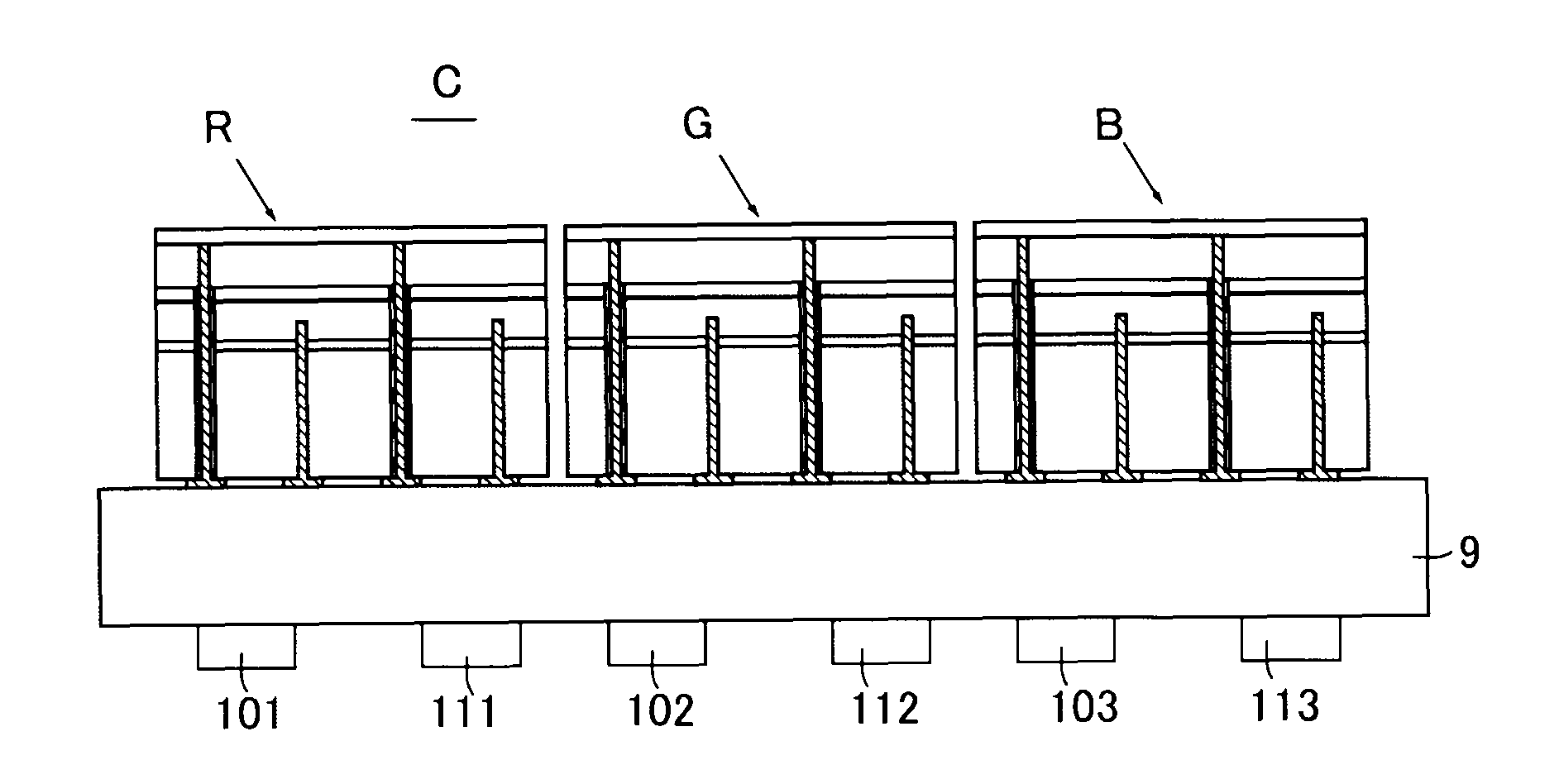
[0074]The light-emitting device according to a second embodiment is illustrated in FIGS. 9 to 11. Referring first to FIGS. 9 and 10, it includes a combination of red, green, and blue light-emitting diodes R, G, B. In this light-emitting device, the light-emitting diodes R, G, B for red, green, and blue being the primary colors of light are combined (as one cell) to obtain white light.

[0075]Each of the red, green, and blue light-emitting diodes R, G, B is the light-emitting diode according to the present invention.

[0076]Referring next to FIG. 11, there is obtained a light-emitting device for white light with a large-area light-emitting surface, wherein the red, green, and blue light-emitting diodes R, G, B are combined as one cell and such cells (C11 to CMN) of the light-emitting diodes are arranged in M columns and N rows.

3. Lighting Apparatus

[0077]A lighting apparatus according to the present invention can be provided using the light-emitting devices shown ...


PUM


Abstract

A light-emitting diode includes a substrate, a semiconductive light-emitting layer, and electrodes. The semiconductive light-emitting layer is deposited on one side of the substrate. The electrodes are composed of a conductive material filled in pores leading to the semiconductive light-emitting layer through the substrate. The semiconductive light-emitting layer includes sequentially deposited n-type and p-type semiconductive layers. The electrodes include n-side and p-side electrodes. One of the n-side and p-side electrodes penetrates through one of the n-type and p-type semiconductive layers, which is disposed closer to the substrate but not targeted for connection, and terminates with a tip thereof located within the other semiconductive layer. The other of the n-side and p-side electrodes penetrates through the substrate from the other side opposite to the one side of the substrate and terminates with a tip thereof located within the one semiconductive layer disposed closer to the substrate.

Description

BACKGROUND OF THE INVENTION[0001]1. Field of the Invention[0002]The present invention relates to a light-emitting diode, and a light-emitting device, a lighting apparatus, a display, and a signal light using the same.[0003]2. Description of the Related Art[0004]Light-emitting diodes have the advantages of energy conservation and long service life and have come to attract attention as a light source of a light-emitting device, a color image display device, a backlight of a liquid crystal panel, or a traffic light.[0005]Taking a blue light-emitting diode as an example, the light-emitting diode has a structure that a buffer layer, an n-type GaN layer, an active layer, a p-type GaN layer, and a transparent electrode layer are sequentially deposited on a substrate made of sapphire, as disclosed in Japanese Unexamined Patent Application Publication No. 2001-210867, for example.[0006]On the transparent electrode layer, partially, there is formed a p-side electrode, while the transparent el...

Claims


Application Information

Patent Timeline
IPC IPC(8): H01L29/18
CPCH01L33/382
Inventor SEKINE, SHIGENOBUSEKINE, YURINAKUWANA, YOSHIHARU
Owner NAPRA
Why Eureka
Try Eureka