Electronic component and electronic-component production method

a technology of electronic components and production methods, applied in the direction of fixed capacitor details, feed-through capacitors, printed circuit non-printed electric components association, etc., can solve the problems of stray capacitance mismatching of the characteristic impedance near the outer electrodes, and reducing the distance between the outer electrodes, so as to prevent the noise of the noise, prevent the characteristic impedance from decreasing, and prevent the effect of stray capacitan

Inactive Publication Date: 2010-11-30
MURATA MFG CO LTD
View PDF13 Cites 34 Cited by
  • Summary
  • Abstract
  • Description
  • Claims
  • Application Information

AI Technical Summary

Benefits of technology

[0015]In this case, it is possible to suppress the stray capacitance produced between adjacent outer electrodes, and to prevent the characteristic impedance from decreasing near the outer electrodes.
[0019]In this case, it is possible to increase the stray capacitance produced between the adjacent outer electrodes, and to reduce the characteristic impedance near the outer electrodes to a desired value.
[0028]As described in detail above, according to the electronic component of the present invention, the magnitude of the stray capacitance produced between the outer electrodes during use of the electronic component corresponds to the dielectric constant of the dielectric layer. Therefore, the magnitude of the stray capacitance produced between the adjacent outer electrodes can be freely controlled by the dielectric constant of the dielectric layer, correspondingly to minimization of the component.
[0029]In particular, the stray capacitance produced between the outer electrodes is suppressed, and the characteristic impedance is prevented from decreasing near the outer electrodes. Therefore, noise is prevented from being caused by the decrease in the characteristic impedance. As a result, a normal operating characteristic can be ensured. Further, the stray capacitance produced between the outer electrodes can be suppressed further, and therefore, the operating characteristic of the electronic component can be improved further.
[0030]In the electronic component according to the present invention, the characteristic impedance near the outer electrodes can be reduced to a desired value. This is considerably convenient.
[0031]In the electronic-component production method, the groove is formed near the exposed end portion of the circuit pattern in the second step so as to prevent the dielectric paste from extending to the exposed end portion in the third step. Therefore, it is possible to produce a high-performance electronic component in which connection failure between the outer electrodes and the circuit patterns is avoided.

Problems solved by technology

However, minimization of the electronic component forcibly reduces the distance between outer electrodes, and this causes a stray capacitance between the outer electrodes.
This stray capacitance may cause mismatching of the characteristic impedance near the outer electrodes.
Mismatching of the characteristic impedance not only deteriorates the differential-signal transmission characteristic in a normal mode, but also changes the differential signal to common-mode noise.
However, this reduces the fixing strength of the outer electrodes to a substrate.
Unfortunately, when the above-described technique disclosed in Patent Document 2 is applied to an electronic component such as a common-mode choke coil, the following problem is caused.

Method used


Image

  • Electronic component and electronic-component production method
  • Electronic component and electronic-component production method
  • Electronic component and electronic-component production method

Examples


first embodiment

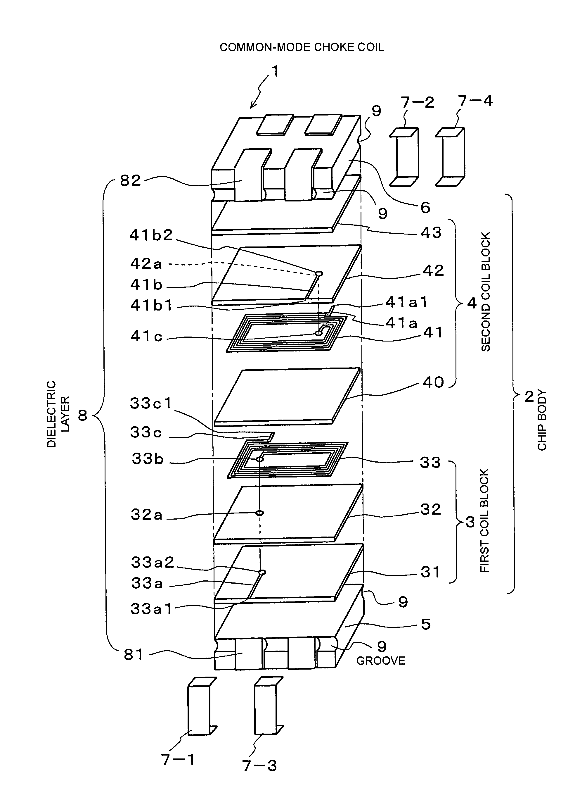
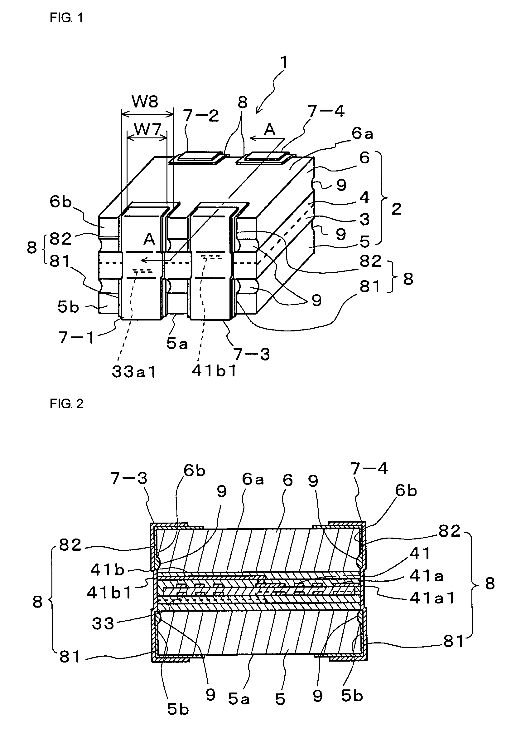
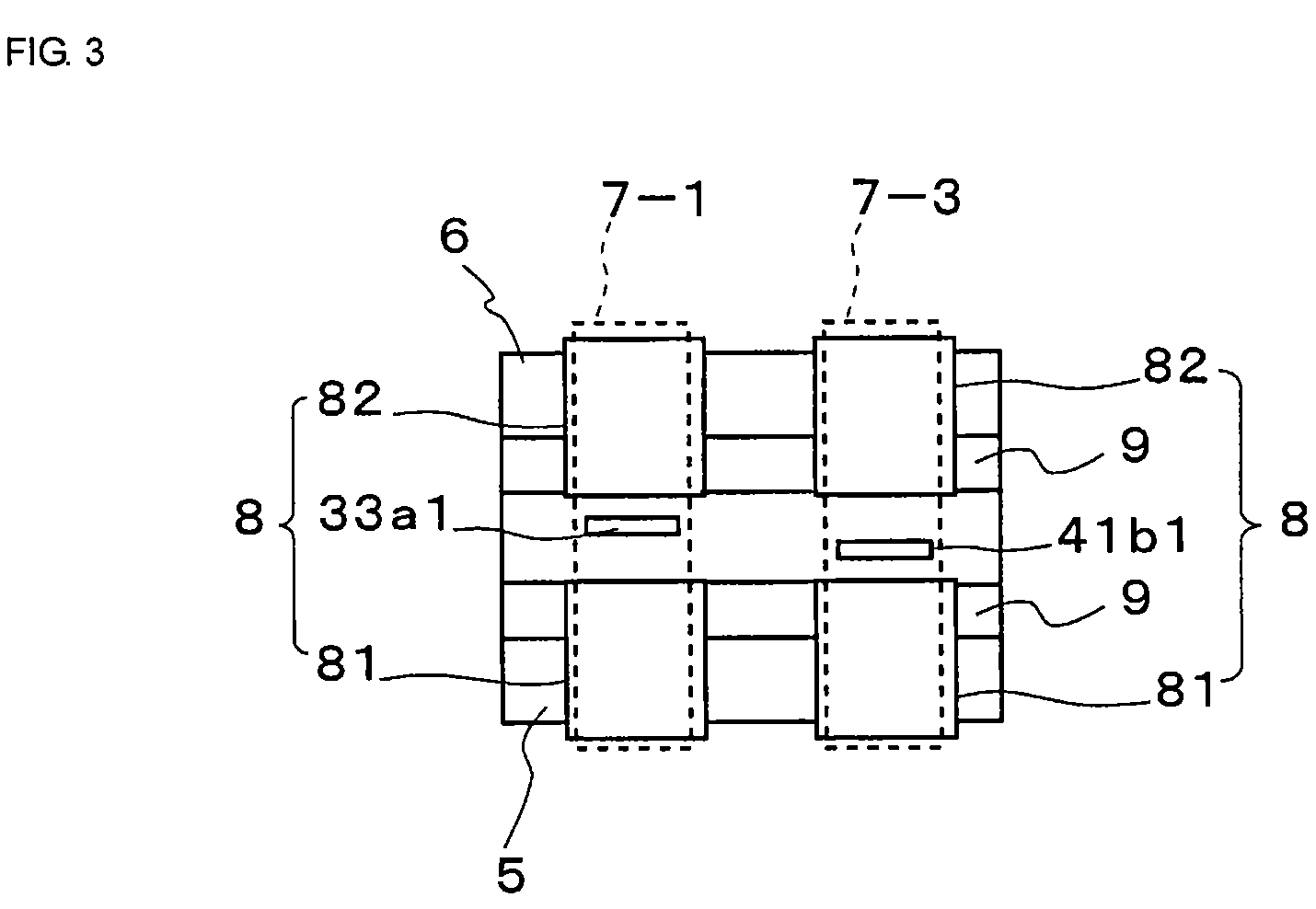
[0048]FIG. 1 is an outside view of an electronic component according to a first embodiment of the present invention, FIG. 2 is a cross-sectional view, as viewed from the directions of arrows A-A in FIG. 1, FIG. 3 is a front view of the electronic component, showing exposed portions of coil patterns, and FIG. 4 is an exploded perspective view of the electronic component.

[0049]An electronic component 1 according to this embodiment is a common-mode choke coil, and includes a chip body 2 and first to fourth outer electrodes 7-1 to 7-4, as shown in FIGS. 1 and 3.

[0050]In the chip body 2, first and second coil blocks 3 and 4 serving as circuit blocks are sandwiched between magnetic substrates 5 and 6 serving as substrate elements from above and below.

[0051]As shown in FIG. 4, the first block 3 includes insulating layers 31 and 32 and a coil pattern 33 that are stacked on the magnetic substrate 5.

[0052]More specifically, the insulating layer 31 is placed on the magnetic substrate 5, and on...

second embodiment

[0091]A second embodiment of the present invention will now be described.

[0092]FIG. 11 is a front view of an electronic component according to a second embodiment of the present invention, and FIG. 12 is a schematic partial sectional view explaining the operation and advantages of the second embodiment.

[0093]The electronic component according to this embodiment is different from the above-described first embodiment in that the characteristic impedance is reduced near the outer electrodes 7-1 to 7-4.

[0094]More specifically, as shown in FIG. 11, a single dielectric layer 8′ that is not split is formed over the adjacent outer electrodes 7-1 and 7-3 (7-2 and 7-4). That is, the single dielectric layer 8′ is provided under the outer electrodes 7-1 and 7-3 (7-2 and 7-4) so as not to cover leading ends 33a1 (33c1) and 41b1 (41a1) of coil patterns 33 and 41, so that the dielectric layer 8′ also lies between the adjacent outer electrodes 7-1 and 7-3 (7-2 and 7-4). The dielectric constant of t...


PUM

PropertyMeasurementUnit
dielectric constantaaaaaaaaaa

Abstract

An electronic component and an electronic-component production method in which the magnitude of a stray capacitance produced between adjacent outer electrodes is controllable. The electronic component includes a chip body and first to fourth outer electrodes. In the chip body, first and second coil block are sandwiched between magnetic substrates. Dielectric layers are interposed between the outer electrodes and the chip body such as to be away from exposed portions of coil patterns in the coil blocks. The dielectric layers have a width larger than a width of the outer electrodes, and a dielectric constant of the dielectric layers is set to be lower than the dielectric constant of the magnetic substrates.

Description

CROSS REFERENCE TO RELATED APPLICATIONS[0001]The present application is a continuation of International Application No. PCT / JP2005 / 021659, filed Nov. 25, 2005, which claims priority to Japanese Patent Application No. JP2005-002115, filed Jan. 7, 2005, the entire contents of each of these applications being incorporated herein by reference in their entirety.FIELD OF THE INVENTION[0002]The present invention relates to an electronic component that can be mounted on an electrical circuit required to have a smaller size and a higher density, and to a production method for the electronic component.BACKGROUND OF THE INVENTION[0003]As this type of electronic component, a chip-type common-mode choke coil is disclosed, for example, in Patent Document 1. A common-mode choke coil is mounted to eliminate noise from a high-speed differential transmission line, and serves to efficiently transmit a differential signal in a normal mode and to eliminate invading noise in a common mode.[0004]With rece...

Claims


Application Information

Patent Timeline
Patent Type & Authority Patents(United States)
IPC IPC(8): H05K7/02H05K7/06H05K7/10H05K7/08
CPCH01F27/027H01F27/292H01G4/35H01G4/40H01F17/0013Y10T29/4916H01G4/30
Inventor KUDO, KAZUHIDEMATSUNAGA, MINORUMATSUTA, KATSUJI
Owner MURATA MFG CO LTD
Why Eureka
Try Eureka