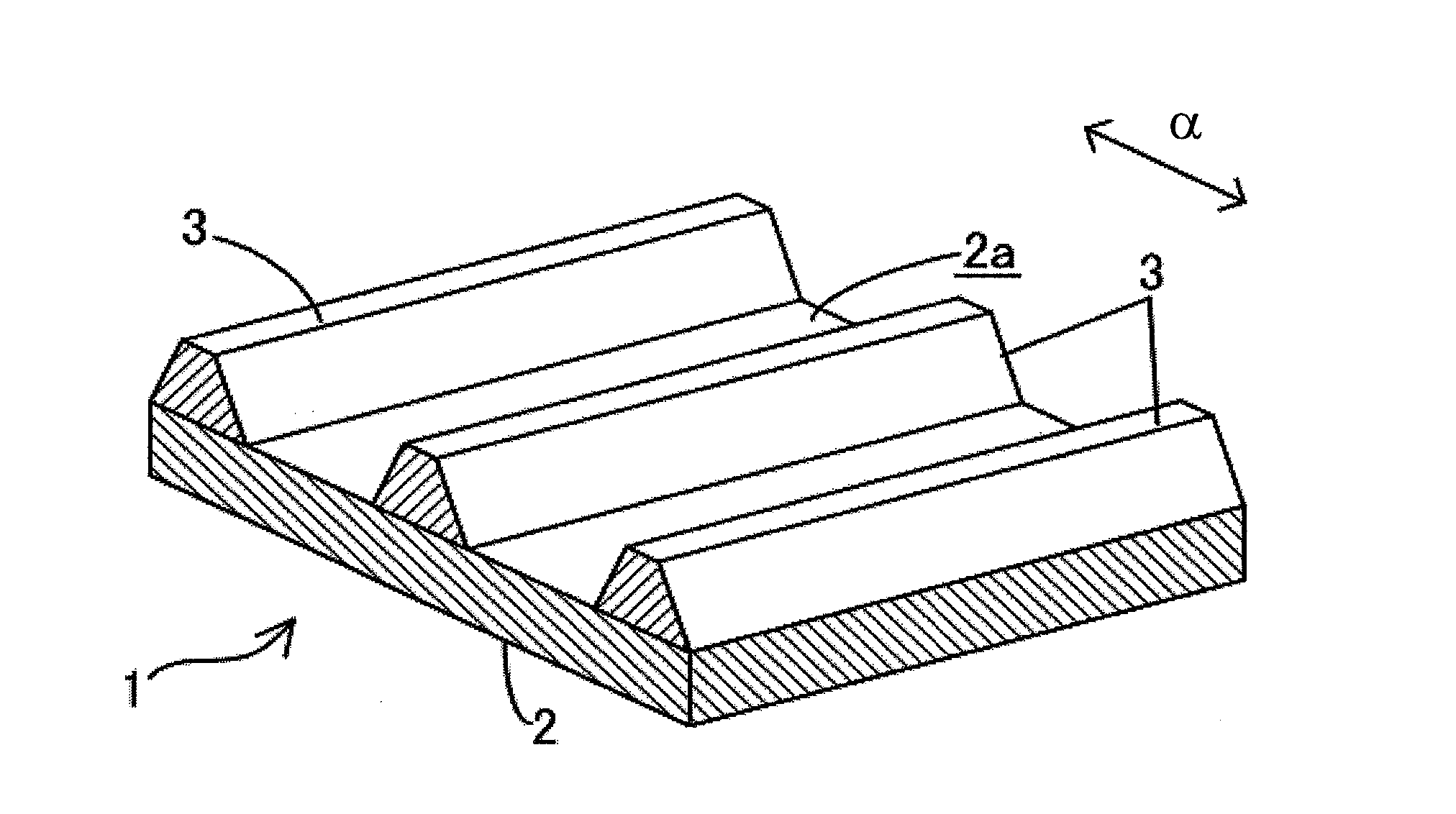
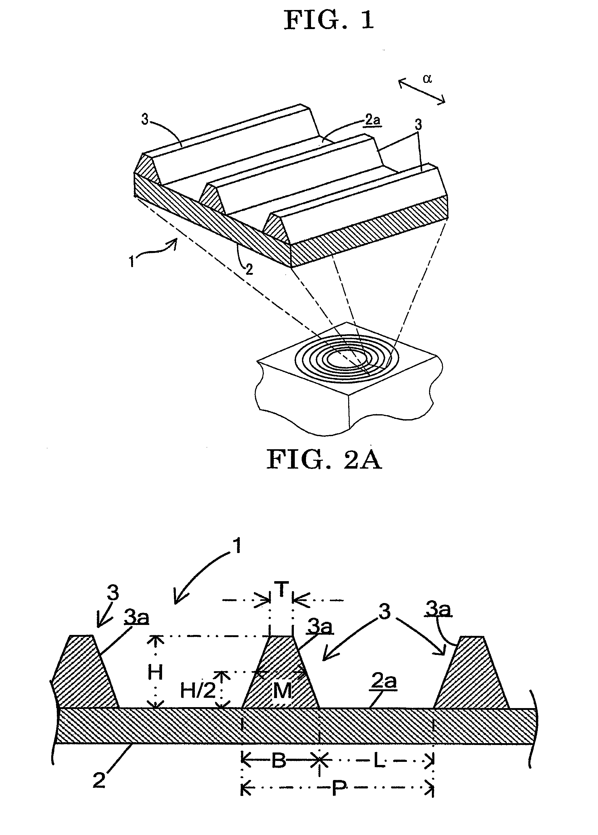
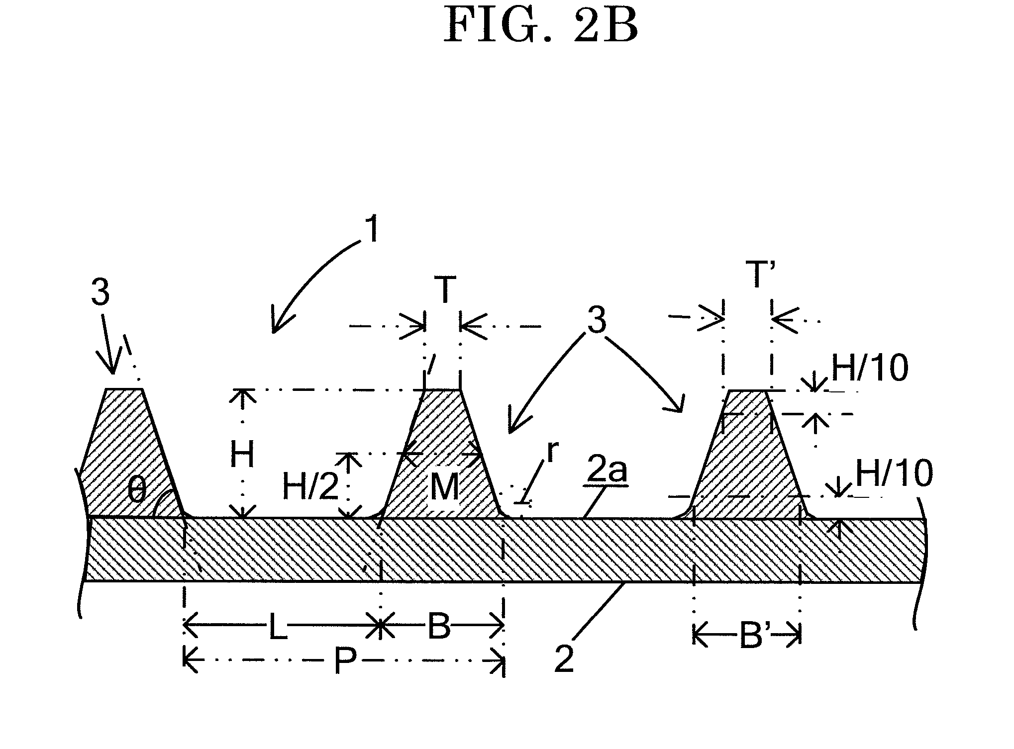
Mold structure

a technology of mold structure and resist layer, applied in the field of mold structure, can solve the problems of inability to obtain an appropriate resist, inability to push out a resist layer, and limit the improvement of surface recording density, so as to achieve efficient transfer of high-quality patterns, less crosstalk, and high signal integrity

Inactive Publication Date: 2010-12-14
FUJIFILM CORP
View PDF36 Cites 6 Cited by
  • Summary
  • Abstract
  • Description
  • Claims
  • Application Information

AI Technical Summary

Benefits of technology

[0013]Specifically, an object of the present invention is to provide a mold structure capable of efficiently transferring a high-quality pattern onto discrete track media and patterned media and forming the pattern thereon, with the use of a nanoimprinting technique.
[0014]Also, another object of the present invention is to provide a mold structure with less crosstalk, etc., capable of transferring a pattern of high signal integrity onto discrete track media and patterned media and forming the pattern thereon.
[0016]According to the present invention, it is possible to solve the problems in related art and to provide a mold structure capable of efficiently transferring a high-quality pattern onto discrete track media and patterned media and forming the pattern thereon, with the use of a nanoimprinting technique.
[0017]Also, according to the present invention, it is possible to provide a mold structure with less crosstalk, etc., capable of transferring a pattern of high signal integrity onto discrete track media and patterned media and forming the pattern thereon.

Problems solved by technology

In order to increase the recording density of hard disk drives, methods such as improvement in the performance of magnetic recording media and reduction in the magnetic head width have been conventionally used; however, as spaces between data tracks are made small, effects of magnetism between adjacent tracks (crosstalk) and effects of heat fluctuation become inevitably great, hence a limitation on improvement in surface recording density by means of the narrowing of magnetic heads or the like.
However, as to a resist pattern forming mold described in JP-A No. 2004-221465, since convex portions formed on a surface thereof are shaped like rectangles in cross-section, it is impossible to push out a resist layer sufficiently when the mold is pressed against the resist layer and thus impossible to obtain an appropriate resist pattern; consequently, the convex portions of the mold structure may possibly vary in height.

Method used


Image

  • Mold structure
  • Mold structure
  • Mold structure

Examples


first embodiment

[0053]FIG. 3 is a cross-sectional view showing a method for producing a mold structure according to a first embodiment. As shown in FIG. 3, first of all, a photoresist solution of PMMA (polymethylmethacrylate), etc. is applied onto an Si (silicon) substrate 10 by means of spin coating or the like, and a photoresist layer 21 is thus formed.

[0054]After that, while the substrate 10 is being rotated, a laser beam (or an electron beam) modulated correspondingly to a servo signal is applied, and a predetermined pattern, for example a pattern corresponding to the servo signal that linearly extends in the radial direction from the rotational center to tracks, is transferred by means of exposure onto portions corresponding to circumferential frames on the whole surface of the photoresist.

[0055]Subsequently, the photoresist layer 21 undergoes a developing process, the exposed portions are removed, then selective etching is conducted in accordance with RIE (reactive ion etching) or the like as...

second embodiment

[0057]FIGS. 4A to 4B are cross-sectional views showing a method for producing a mold structure according to a second embodiment. As shown in FIG. 4A, first of all, a photoresist solution of PMMA, etc. is applied onto an Si (silicon) substrate 10 by means of spin coating or the like, and a photoresist layer 21 is thus formed.

[0058]After that, while the substrate 10 is being rotated, a laser beam (or an electron beam) modulated correspondingly to a servo signal is applied, and a predetermined pattern, for example a pattern corresponding to the servo signal that linearly extends in the radial direction from the rotational center to tracks, is transferred by means of exposure onto portions corresponding to circumferential frames on the whole surface of the photoresist.

[0059]Subsequently, the photoresist undergoes a developing process, the exposed portions are removed, then selective etching is conducted in accordance with RIE or the like as the photoresist pattern serves as a mask, and ...

third embodiment

[0065]FIG. 5 is a cross-sectional view showing a method for producing a mold structure according to a third embodiment. As shown in FIG. 5, first of all, a photoresist solution of PMMA, etc. is applied onto a quartz substrate 30 by means of spin coating or the like, and a photoresist layer 21 is thus formed.

[0066]After that, while the quartz substrate 30 is being rotated, a laser beam (or an electron beam) modulated correspondingly to a servo signal is applied, and a predetermined pattern, for example a pattern corresponding to the servo signal that linearly extends in the radial direction from the rotational center to tracks, is transferred by means of exposure onto portions corresponding to circumferential frames on the whole surface of the photoresist.

[0067]Subsequently, the photoresist layer 21 undergoes a developing process, the exposed portions are removed, then selective etching is conducted in accordance with RIE or the like as the pattern of the photoresist layer 21 after t...


PUM

PropertyMeasurementUnit
width roughnessaaaaaaaaaa
aspect ratioaaaaaaaaaa
45°≦θaaaaaaaaaa

Abstract

There is provided a mold structure containing a substrate, and a plurality of convex portions formed in the shape of concentric circles at predetermined intervals on one surface of the substrate, wherein a cross-sectional shape of the convex portions with respect to a radial direction of the concentric circles is such that a middle width M of each of the convex portions with respect to a heightwise direction is greater than a width T of a top portion of each of the convex portions with respect to the radial direction of the concentric circles.

Description

BACKGROUND OF THE INVENTION[0001]1. Field of the Invention[0002]The present invention relates to a mold structure provided with a pattern of concavities and convexities for transferring information onto a magnetic recording medium, in particular a mold structure for nanoimprinting.[0003]2. Description of the Related Art[0004]In recent years, hard disk drives that are superior in reading and writing swiftness and costs have begun being incorporated in portable devices such as cellular phones, compact acoustic devices and video cameras as major storage devices, and a technique for improving recording density has been required to meet the demand for further reduction in size and enlargement in capacity.[0005]In order to increase the recording density of hard disk drives, methods such as improvement in the performance of magnetic recording media and reduction in the magnetic head width have been conventionally used; however, as spaces between data tracks are made small, effects of magne...

Claims


Application Information

Patent Timeline
Patent Type & Authority Patents(United States)
IPC IPC(8): B29D17/00
CPCB82Y10/00B82Y40/00G03F7/0002G11B5/743G11B5/855Y10S425/81
Inventor USA, TOSHIHIROICHIKAWA, KENJIKOMATSU, KAZUNORI
Owner FUJIFILM CORP
Why Eureka
Try Eureka