Direct die attach utilizing heated bond head

a technology of heat-sealed bonding and die-attaching head, which is applied in the direction of solid-state devices, manufacturing tools, and so on, which can solve the problems of reducing the efficiency of the process,

Active Publication Date: 2010-12-21
ASMPT SINGAPORE PTE LTD
View PDF10 Cites 101 Cited by
  • Summary
  • Abstract
  • Description
  • Claims
  • Application Information

AI Technical Summary

Benefits of technology

[0007]It is thus an object of the invention to seek to provide a direct die attach method for die bonding which avoids at least some of the aforesaid shortcomings of prior art die bonding methods.

Problems solved by technology

Although silver epoxy bonding is a simple and mature process, its low thermal conductivity has limited its application in high power applications.
The flip chip structure has the drawback of having a relatively small contact area for effective heat dissipation.
However, there are some problems which retard the effectiveness of the process.
Of most concern is flux residue, which might lead to package reliability issues due to moisture corrosion.
Furthermore, chip movement including die tilting and die rotation cannot be avoided due to the difficulty of controlling the flux dispensing volume and uniformity with precision.
Insufficient flux induces non-wetting of the gold-tin material, but using too much flux causes poor wetting of the gold-tin material and affects placement accuracy.
However, two issues have emerged recently for direct die attachment during the manufacture of HBLED devices.
Firstly, due to the slow solidification rate of the thick gold-tin layer, the squeezed out solder tends to flow back after the bond head is removed from the chip surface, and voids may appear at the interface between LED and the substrate after bonding.
The voids are unacceptable, since the reliability of packaged electronics strongly depends on the die attach quality, and any void or a small delamination may cause instant temperature increase in the die, leading sooner or later to failure in the package.
It will take a significant amount of time to finish bonding LEDs onto the whole substrate, and the LEDs already bonded will endure a longer annealing time on the heated substrate, which will degrade the LED performance.

Method used


Image

  • Direct die attach utilizing heated bond head
  • Direct die attach utilizing heated bond head
  • Direct die attach utilizing heated bond head

Examples


Embodiment Construction

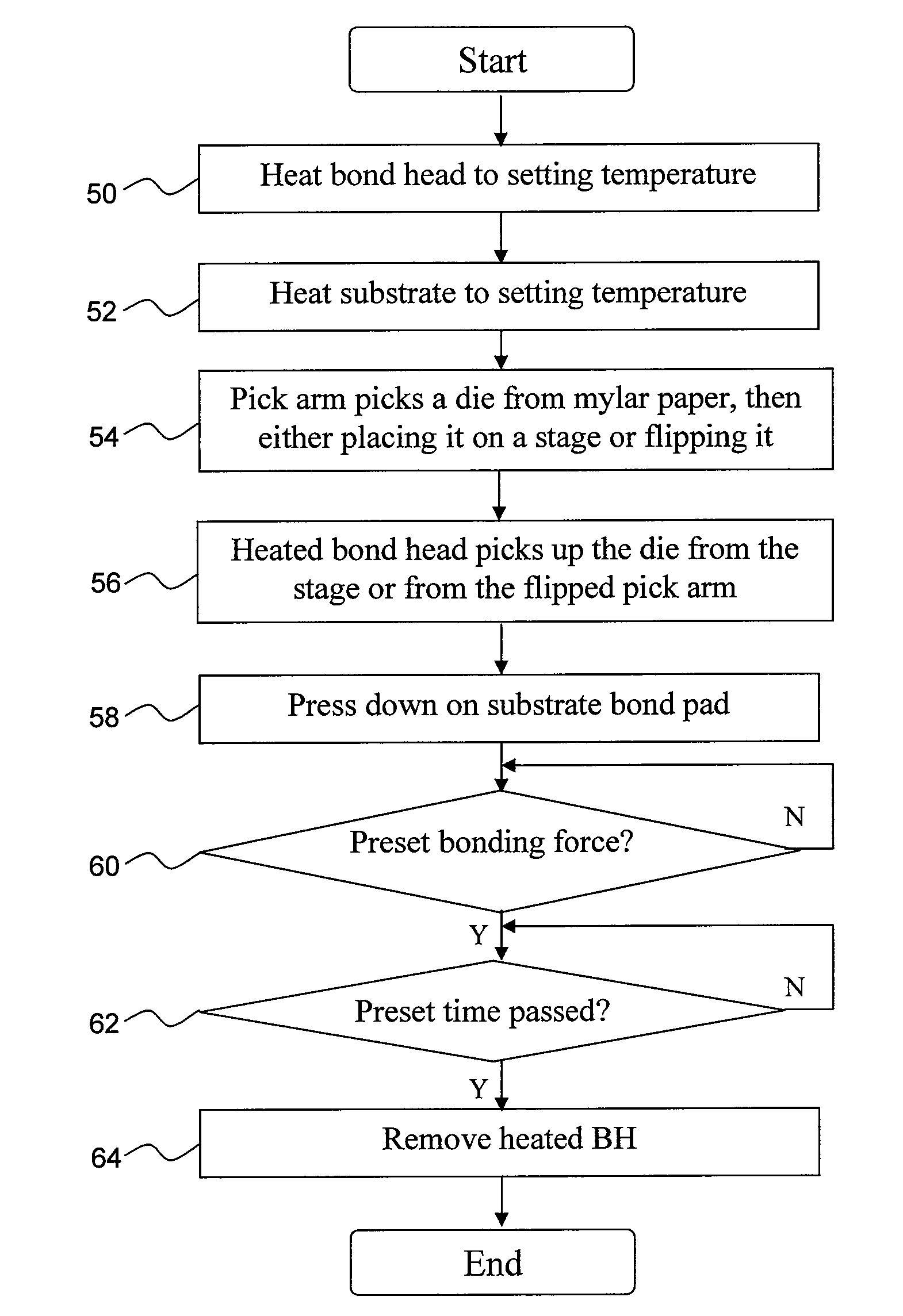
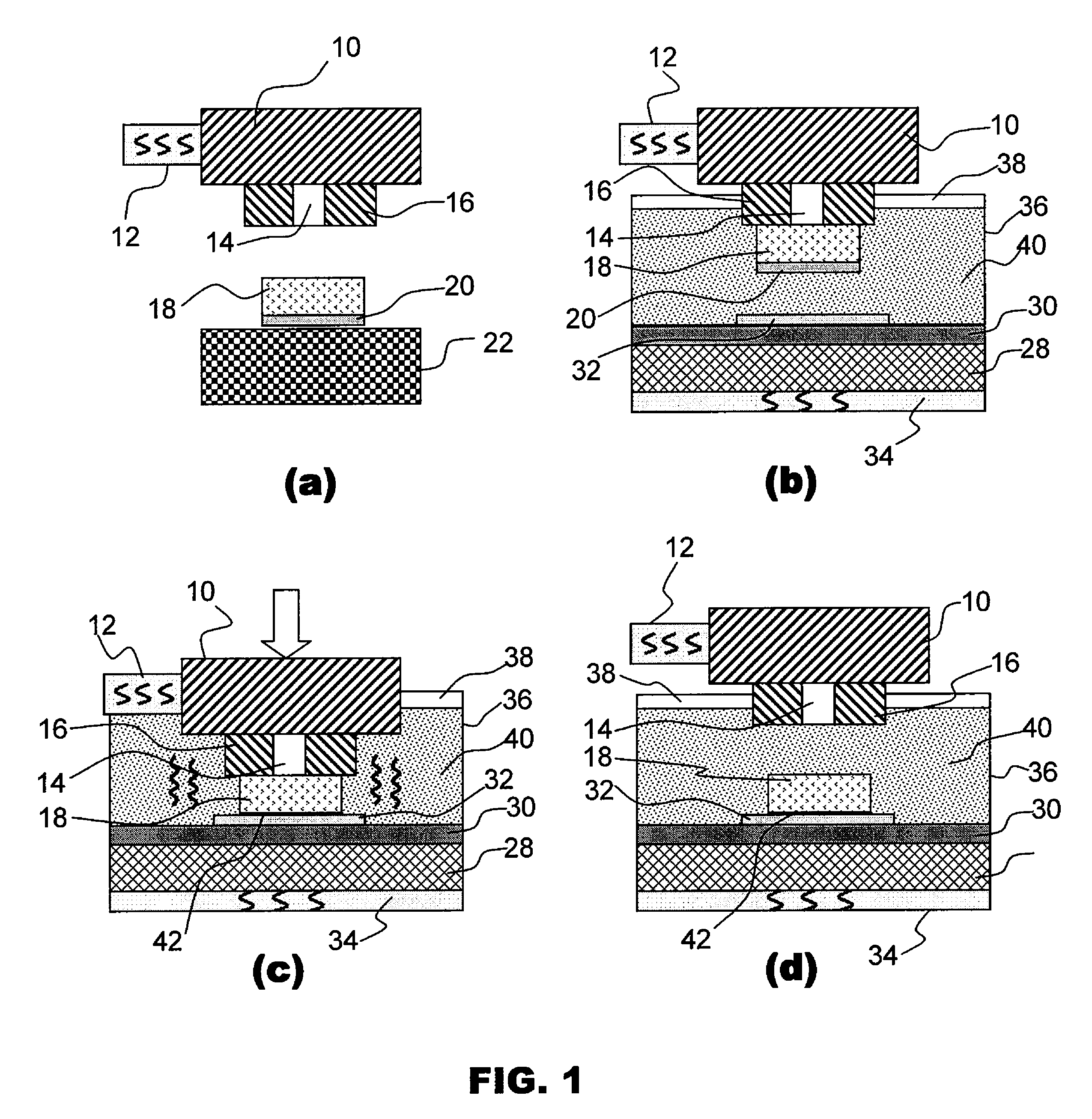
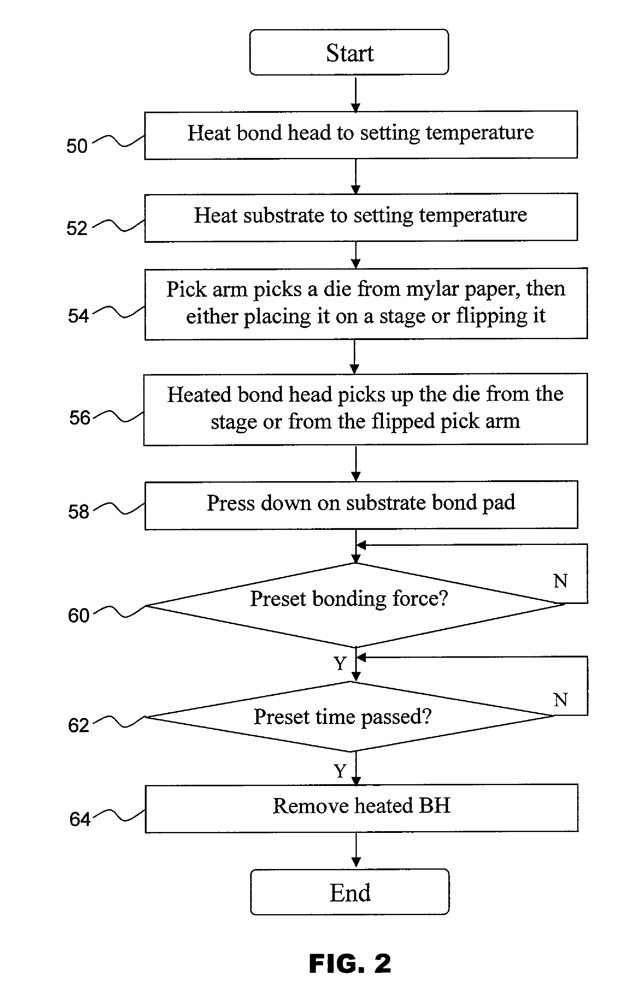
[0014]FIGS. 1(a) to 1(d) illustrate schematic side views of a die bonding operation according to the preferred embodiment of the invention successively demonstrating the process steps for mounting a die onto a substrate.

[0015]In FIG. 1(a), a bond head 10 is first heated to a bond head setting temperature, T1. The bond head 10 in the present embodiment has a heating element 12 and a vacuum system associated with it. The vacuum system (not shown) is used to maintain a negative pressure in the suction hole 14 of the die collet 16. The dimension of the suction hole 14 is less than the size of a die 18, which may be a High Brightness or other LED chip. Heat generated from the heating element 12 of the bond head 10 is conducted to the die collet 16 and subsequently to the die 18 when the bond head 10 is holding the die 18 by collet suction.

[0016]The die 18 comprises a solder layer, such as eutectic layer 20 at its bottom, which has a melting point Tm. The bond head setting temperature T1 ...


PUM

PropertyMeasurementUnit
bond head setting temperature T1aaaaaaaaaa
setting temperature T2aaaaaaaaaa
melting point Tmaaaaaaaaaa

Abstract

A method is provided for bonding a die comprising a solder layer which has a melting point Tm. A bond head is heated to a bond head setting temperature T1, which is higher than Tm, and a substrate is heated to a substrate setting temperature T2, which is lower than Tm. The bond head then picks up the die and heats the die towards temperature T1 so as to melt the solder layer. The solder layer of the die is pressed onto the substrate so as to bond the die to the substrate, and thereafter the bond head is separated from the die so that the solder layer is cooled towards T2 and solidifies.

Description

FIELD OF THE INVENTION[0001]The invention relates to the bonding of semiconductor dice or chips, such as light-emitting diodes (LEDs), onto a substrate.BACKGROUND AND PRIOR ART[0002]For die bonding during the assembly of electronic packages, a robust die attach process is critical to achieve low electrical resistance, low thermal resistance and good mechanical and electrical integrity. The existing die bonding processes for High Brightness LED (HBLED) devices typically involve silver (Ag) epoxy bonding, gold-tin (AuSn) eutectic bonding, thermosonic (TS) bonding with gold (Au) studs or solder reflow with solder bumps for flip chip bonding. Although silver epoxy bonding is a simple and mature process, its low thermal conductivity has limited its application in high power applications. The flip chip structure has the drawback of having a relatively small contact area for effective heat dissipation. Among these die bonding methods, gold-tin eutectic bonding offers the advantages of low ...

Claims


Application Information

Patent Timeline
Patent Type & Authority Patents(United States)
IPC IPC(8): B23K31/02
CPCH01L24/83H01L24/75H01L24/29H01L2224/29144H01L2924/12041H01L2224/83191H01L2224/838H01L2924/01033H01L2924/01046H01L2924/01047H01L2924/0105H01L2924/01079H01L2924/01082H01L2924/3025H01L2224/32506H01L2224/29111H01L2924/15787H01L2924/157H01L2924/0132H01L2224/29101H01L2924/0665H01L2924/014H01L2924/01322H01L2924/01006H01L2924/01005H01L2224/2919H01L2924/00H01L2924/00014H01L21/50
Inventor LI, MINGDING, YINGTU, PING LIANGLO, KING MINGCHUNG, KWOK KEE
Owner ASMPT SINGAPORE PTE LTD
Why Eureka
Try Eureka