Application specific solar cell and method for manufacture using thin film photovoltaic materials

a technology of photovoltaic materials and solar cells, applied in the field of photovoltaic materials, can solve the problems of wasting energy, reducing the efficiency of solar energy conversion, and reducing the efficiency of sunlight conversion into electrical power, so as to achieve easy control and automation of laser beam scanning operations, and improve the efficiency of sunlight conversion. , the effect of increasing the efficiency of sunlight conversion

Active Publication Date: 2010-12-21
CM MFG
View PDF27 Cites 62 Cited by
  • Summary
  • Abstract
  • Description
  • Claims
  • Application Information

AI Technical Summary

Benefits of technology

[0012]Depending upon the specific embodiment, one or more of these features may also be included. The present technique provides an easy to use process that relies upon conventional technology that is nanotechnology based. In some embodiments, the method may provide a thin film based solar module with higher efficiencies in converting sunlight into electrical power using a multiple junction design and method. Depending upon the embodiment, the efficiency can be about 10 percent or 20 percent or greater. Additionally, the method provides a process that is compatible with conventional process technology without substantial modifications to conventional equipment and processes. For example, a pulse laser systems with a homogenous top-hat beam profiles are readily available commercially and laser beam scanning operation can be easily controlled and automated. Depending on the film material that to be removed selectively, the laser characteristics including the wavelength, power level, pulse length and duration etc. can be adjusted accordingly. In a specific embodiment, the present method and system can also be provided using large scale and environmentally friendly manufacturing techniques, which eliminate the usage of solvent for cleaning the side surface and reduce running costs associated with the manufacture of the photovoltaic devices. In particular, the side surface the thin film photovoltaic devices exposed after laser separation process is completely cleaned without any shorting between layers of the thin film. In another specific embodiment, the present method and structure can also be provided using any combination of suitable single junction solar cell designs to form top and lower cells, although there can be more than two stacked cells depending upon the embodiment. In a preferred embodiment, the present method and system allows for design of a custom application specific solar module using application software to provide instructions for design and manufacture processes. Embodiments of the invention provide big advantages for volume manufacturing custom solar module with substantially reduced cost. Depending upon the embodiment, one or more of these benefits may be achieved. These and other benefits will be described in more throughout the present specification and more particularly below.

Problems solved by technology

Unfortunately, petrochemical energy is limited and essentially fixed based upon the amount available on the planet Earth.
Additionally, as more human beings begin to drive and use petrochemicals, it is becoming a rather scarce resource, which will eventually run out over time.
Although solar energy is clean and has been successful to a point, there are still many limitations before it becomes widely used throughout the world.
Crystalline materials are often costly and difficult to make on a wide scale.
Additionally, devices made from such crystalline materials have low energy conversion efficiencies.
Similar limitations exist with the use of thin film technology in making solar cells.
That is, efficiencies are often poor.
Additionally, film reliability is often poor and cannot be used for extensive periods of time in conventional environmental applications.
Although somewhat successful, it is often difficult to match currents between upper and lower solar cells.
Furthermore, solar cells often come in standard designs and are often difficult to customize, which is a further limitation.

Method used


Image

  • Application specific solar cell and method for manufacture using thin film photovoltaic materials
  • Application specific solar cell and method for manufacture using thin film photovoltaic materials
  • Application specific solar cell and method for manufacture using thin film photovoltaic materials

Examples


Embodiment Construction

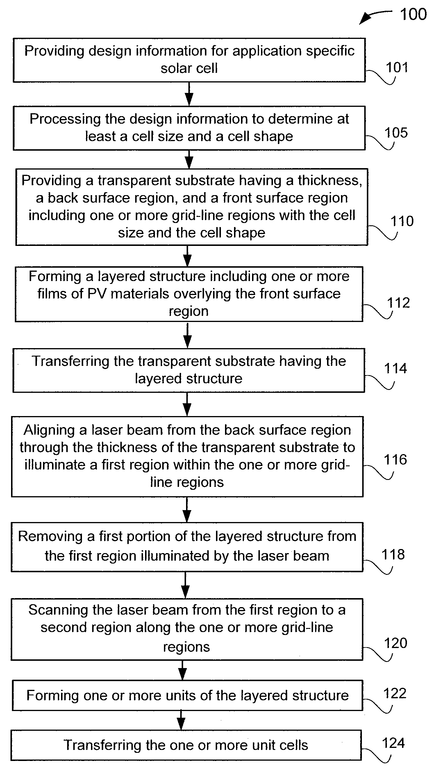
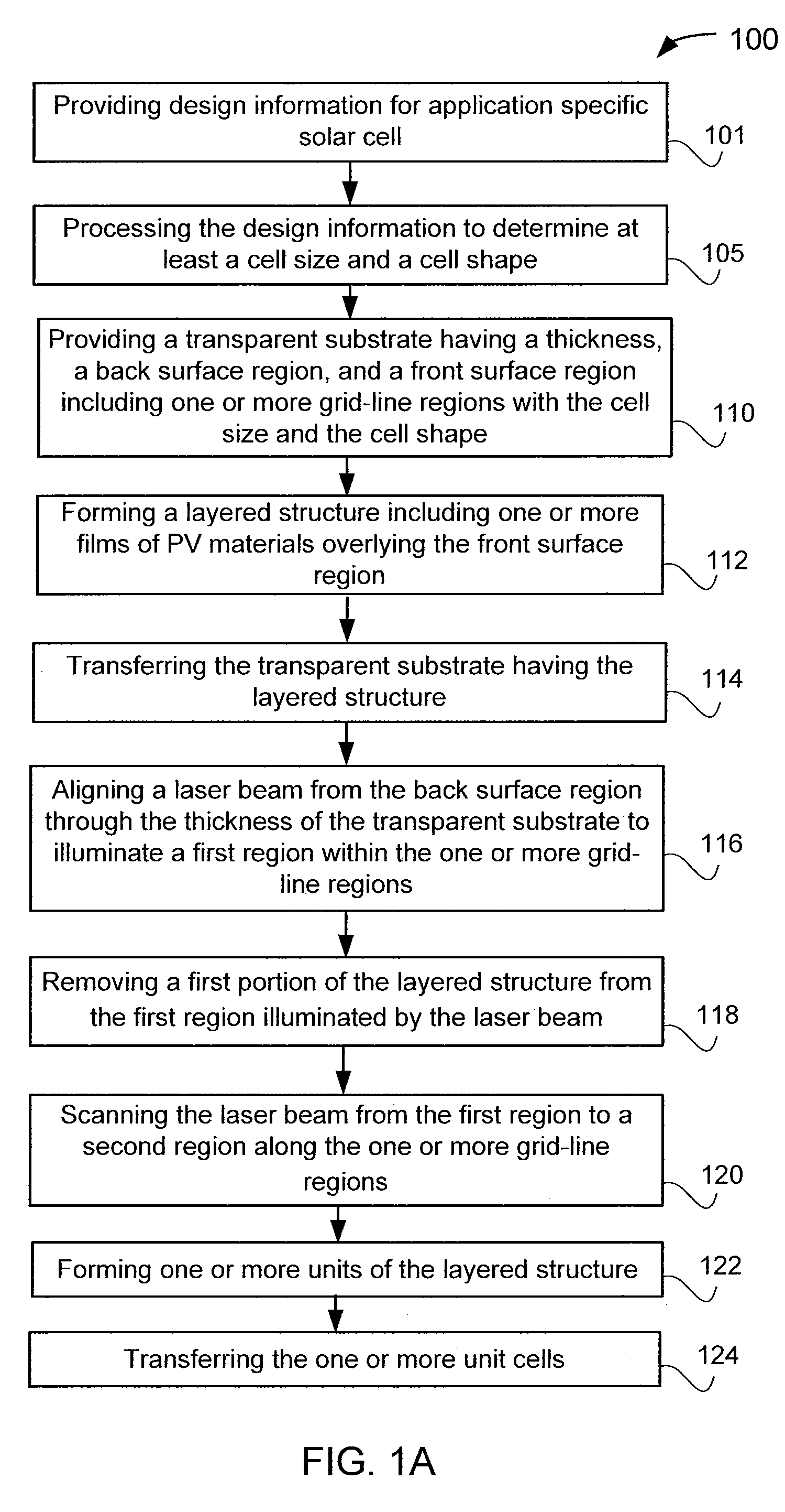
[0023]The present invention relates generally to photovoltaic materials. More particularly, the present invention provides a method and system for design and manufacture of a solar module using a laser separation process for forming one or more unit cells from continuous layered structure of photovoltaic materials. Merely by way of example, the present method and structure have been implemented to manufacture an application specific thin film solar cell having single or multi junction photovoltaic materials, but it would be recognized that the invention may have other configurations.

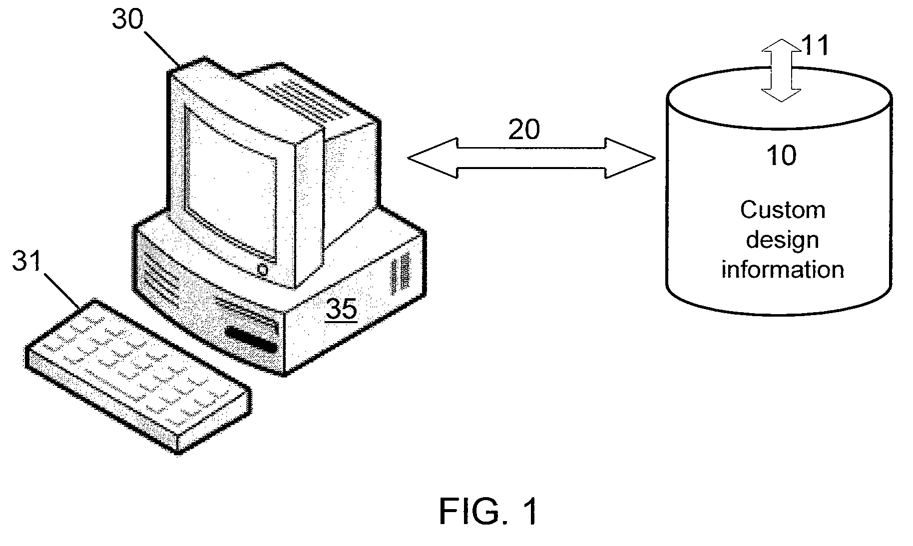
[0024]FIG. 1 is a simplified diagram illustrating a computer configured to receive a custom design information stored in a database according to an embodiment of the present invention. This diagram is merely an example, which should not unduly limit the scope of the claims herein. As shown, a database 10 is established for storing a plurality of custom design information data. In one embodiment, the data...


PUM


Abstract

A method for manufacture of application specific solar cells includes providing and processing custom design information to determine at least a cell size and a cell shape. The method includes providing a transparent substrate having a back surface region, a front surface region, and one or more grid-line regions overlying the front side surface region. The one or more grid regions provide one or more unit cells having the cell size and the cell shape. The method further includes forming a layered structure including photovoltaic materials overlying the front surface region. Additionally, the method includes aligning a laser beam from the back surface region to illuminate a first region within the one or more grid-line regions, subjecting a first portion of the layered structure overlying the first region to the laser beam to separate the first portion of the layered structure from the first region, and scanning the laser beam along the one or more grid-line regions to cause formation of one or more unit cells having the cell size and cell shape. The method further includes transferring the one or more unit cells.

Description

CROSS-REFERENCES TO RELATED APPLICATIONS[0001]This application claims priority to U.S. Provisional Patent Application No. 61 / 095,939, filed Sep. 10, 2008, entitled “APPLICATION SPECIFIC SOLAR CELL AND METHOD FOR MANUFACTURE USING THIN FILM PHOTOVOLTAIC MATERIALS” by inventors Chester A. Farris, III and Albert S. Brown, commonly assigned and incorporated by reference herein for all purposes.BACKGROUND OF THE INVENTION[0002]The present invention relates generally to photovoltaic materials. More particularly, the present invention provides a method and system for design and manufacture of a solar module using a laser separation process for forming one or more unit cells from continuous layered structure of photovoltaic materials. Merely by way of example, the present method and structure have been implemented to an application specific thin film solar cell having single or multi-junction photovoltaic materials, but it would be recognized that the invention may have other configurations...

Claims


Application Information

Patent Timeline
Patent Type & Authority Patents(United States)
IPC IPC(8): H01L21/00
CPCH01L27/1446H01L27/1443
Inventor FARRIS, III, CHESTER A.BROWN, ALBERT S.
Owner CM MFG
Why Eureka
Try Eureka