Optical information recording medium
a technology of optical information and recording medium, applied in the direction of instruments, photomechanical devices, transportation and packaging, etc., can solve the problems of heat accumulation jitter property degrade, etc., and achieve the effect of superior modulation and superior jitter property
- Summary
- Abstract
- Description
- Claims
- Application Information
AI Technical Summary
Benefits of technology
Problems solved by technology
Method used
Image
Examples
example 1
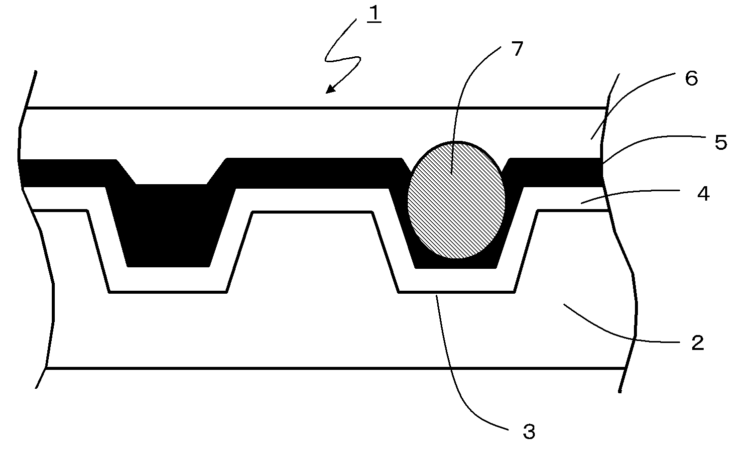
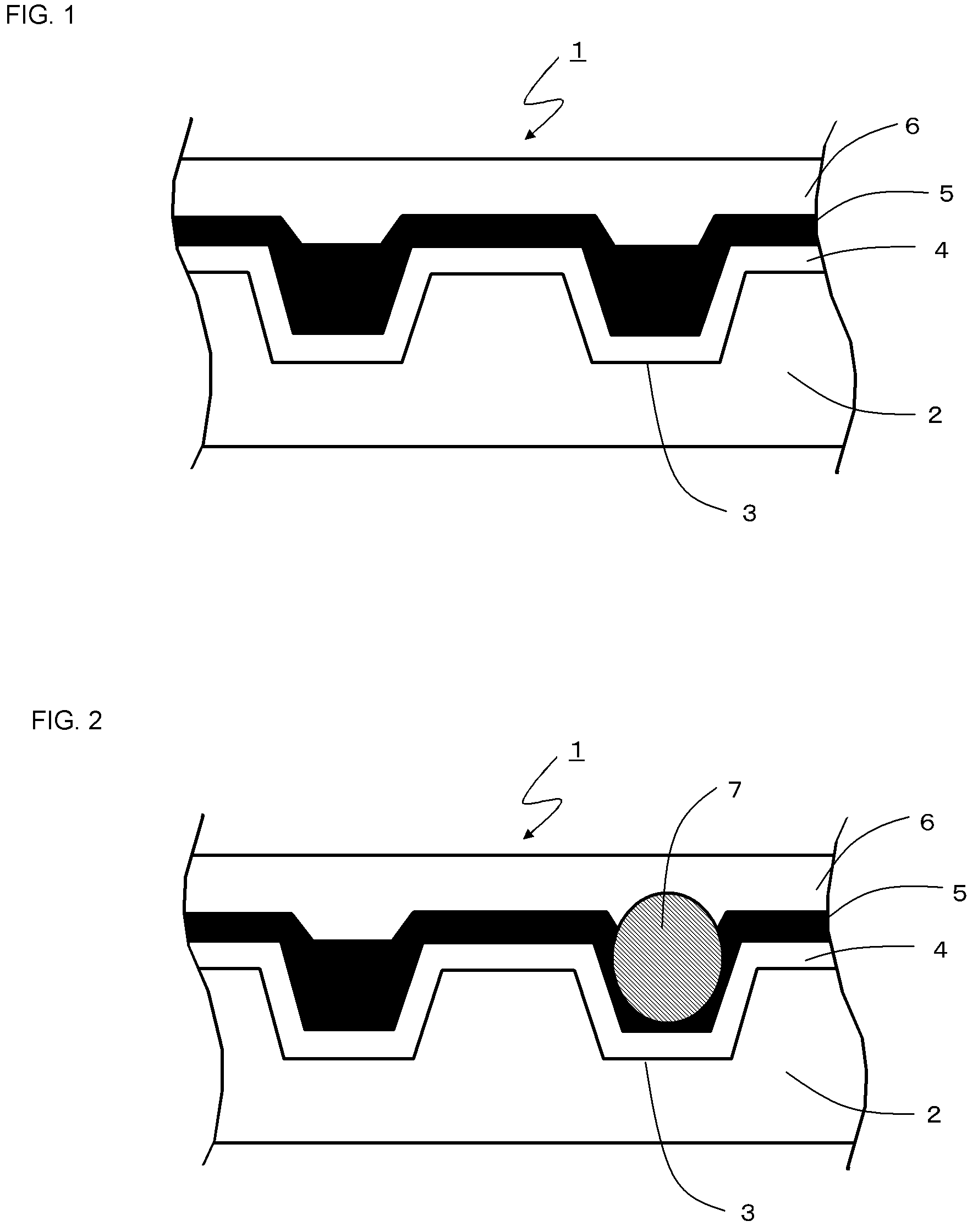
[0051]A disc-shaped substrate made of polycarbonate having an outer diameter of 120 mm and a thickness of 1.1 mm was formed by injection molding to have a penetrating hole in a central portion and a pre-groove having a track pitch of 0.32 μm. On the surface in which the pre-groove was formed, a reflection layer having a thickness of 100 nm was formed by sputtering using a Ag alloy. Subsequently, a dye solution containing a TFP solvent and an azo-based dye shown formula (1) was applied by a spin coating method, followed by drying at 80° C. for 30 minutes, thereby forming a recording layer. By the steps as described above, a plurality of samples necessary for evaluation was prepared.
[0052]
[0053]wherein in the figure, A and A′ each indicate a heterocyclic ring containing at least one hetero atom selected from the group consisting of a nitrogen, an oxygen, a sulfur, a selenium, and a tellurium atom, and may be the same or may be different from each other; R21 to R24 each independently i...
example 2
[0058]A disc-shaped substrate made of polycarbonate having an outer diameter of 120 mm and a thickness of 1.1 mm was formed by injection molding to have a penetrating hole in a central portion and a pre-groove having a track pitch of 0.32 μm. On the surface in which the pre-groove was formed, a reflection layer having a thickness of 100 nm was formed by sputtering using a Ag alloy. Subsequently, a dye solution containing a TFP solvent and an azo-based dye shown in formula (1) (the same as in Example 1) was applied by a spin coating method, followed by drying at 80° C. for 30 minutes, thereby forming a recording layer. By the steps as described above, a plurality of samples necessary for evaluation was prepared.
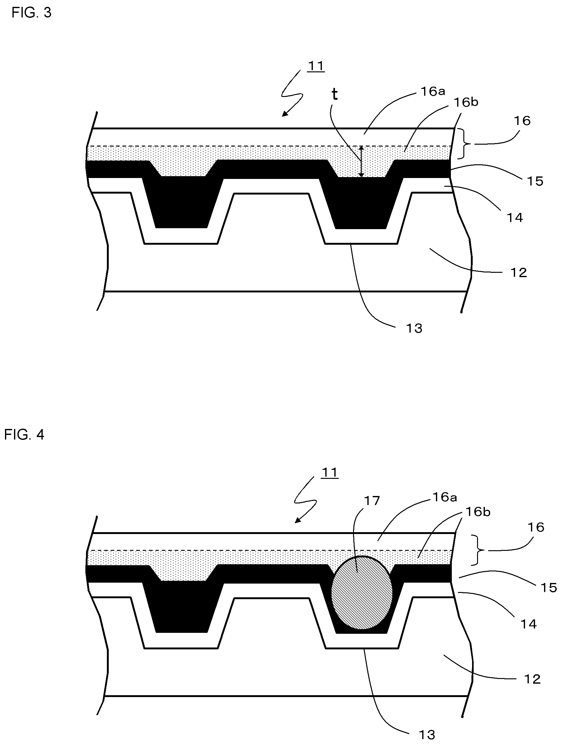
[0059]Next, protective layers having a thickness of 0.5 μm were formed on the above samples by sputtering using light transmissive protective layer materials having different elastic-plastic deformation ratios. The sputtering was performed by S-100W, manufactured by Shibaura M...
PUM
| Property | Measurement | Unit |
|---|---|---|
| elastic modulus | aaaaa | aaaaa |
| thickness | aaaaa | aaaaa |
| diameter | aaaaa | aaaaa |
Abstract
Description
Claims
Application Information


