Electronic circuit, electro-optical device, and electronic apparatus including the same

a technology of electrooptical devices and electronic devices, applied in the direction of static indicating devices, optical radiation measurement, instruments, etc., can solve the problems of a/d conversion potential significantly narrow dynamic range, poor saturation characteristics of polysilicon thin-film transistors, etc., to achieve optimal display quality, increase in cost, and sufficient a/d conversion dynamic range

Inactive Publication Date: 2011-01-11
JAPAN DISPLAY WEST
View PDF14 Cites 9 Cited by
  • Summary
  • Abstract
  • Description
  • Claims
  • Application Information

AI Technical Summary

Benefits of technology

[0037]An advantage of some aspects of the invention is that an A / D conversion circuit including polysilicon thin-film transistors is provided in which a sufficient A / D conversion dynamic range can be obtained and which is suitable for polysilicon thin-film transistors.
[0040]In the electronic circuit, according to the above aspect of the invention, preferably, any one of the following structures is used: a structure in which the storage circuit includes a first capacitive element and a second capacitive element, and either one or both of the first capacitive element and the second capacitive element are electrically connected to the sensor in response to a range-switching signal; a structure in which the storage circuit includes the first capacitive element, the second capacitive element, and a first switching element, and the first switching element writes a reset voltage into the first capacitive element at an appropriate timing, and the reset voltage changes in response to the range-switching signal; and a structure in which the storage circuit includes a capacitive transistor having an active layer made of thin-film polysilicon, the range-switching signal is connected to a source electrode and a drain electrode of the capacitive transistor, and an end of the sensor is connected to a gate electrode of the capacitive transistor. In such a structure, it is possible to realize the switching of the range by means of a simple circuit configuration.
[0041]Furthermore, in the electronic circuit, preferably, the sensor is a PIN junction diode or a PN junction diode including an active layer made of thin-film polysilicon, the active layer being the same layer as the active layer of the capacitive transistor, and the measured quantity corresponds to a light illuminance. In such a structure, it is possible to measure the illuminance of light with which the substrate is irradiated without an increase in cost. For example, when the electronic circuit is applied to a display device, it is possible to maintain optimal display quality in response to external light.
[0042]Furthermore, in the electronic circuit, preferably, the sensor is a resistor including the thin-film polysilicon which is the same as that for the active layer of the capacitive transistor, and the measured quantity corresponds to a temperature. In such a structure, it is possible to measure the temperature of the substrate without an increase in cost. For example, when the electronic circuit is applied to a display device, it is possible to control gradations optimally so that optimal display quality is maintained in response to temperature.
[0043]Furthermore, in the electronic circuit, preferably, the voltage detection circuit includes a plurality of comparator circuits having the same circuit configuration, and different reference voltages are applied to the comparator circuits. Alternatively, preferably, the voltage detection circuit includes a plurality of CMOS inverters having different ratios of the channel width of an N-channel transistor to the channel width of a P-channel transistor. In such a structure, it is possible to further increase the dynamic range in which A / D conversion can be performed.
[0044]Other aspects of the invention relate to an electro-optical device including any of the electronic circuits described above and an electronic apparatus including the electro-optical device. In such a structure, since an A / D conversion circuit can be formed on a glass substrate in the same manufacturing step as an active matrix, it is possible to manufacture an electro-optical device with a built-in sensor at low cost. By incorporating the electro-optical device into an electronic apparatus, it is possible to manufacture a multifunctional electronic apparatus excellent in display quality at lower cost. Furthermore, since the freedom with which the sensor can be arranged is enhanced, the overall dimensions can be reduced, and it is possible to manufacture an electronic apparatus with excellent design properties, which is also advantageous.

Problems solved by technology

However, in general, characteristics, in particular, saturation characteristics, of polysilicon thin-film transistors are inferior to those of MOS transistors which are formed on single-crystal silicon substrates.
Therefore, polysilicon thin-film transistors have a problem in that the dynamic range where A / D conversion is possible is significantly narrow.
As described above, in the A / D conversion circuit including polysilicon thin-film transistors, it is not possible to obtain a sufficient A / D conversion dynamic range compared with the case in which MOS transistors on a single-crystal silicon device are used, which is a problem.

Method used


Image

  • Electronic circuit, electro-optical device, and electronic apparatus including the same
  • Electronic circuit, electro-optical device, and electronic apparatus including the same
  • Electronic circuit, electro-optical device, and electronic apparatus including the same

Examples


first embodiment

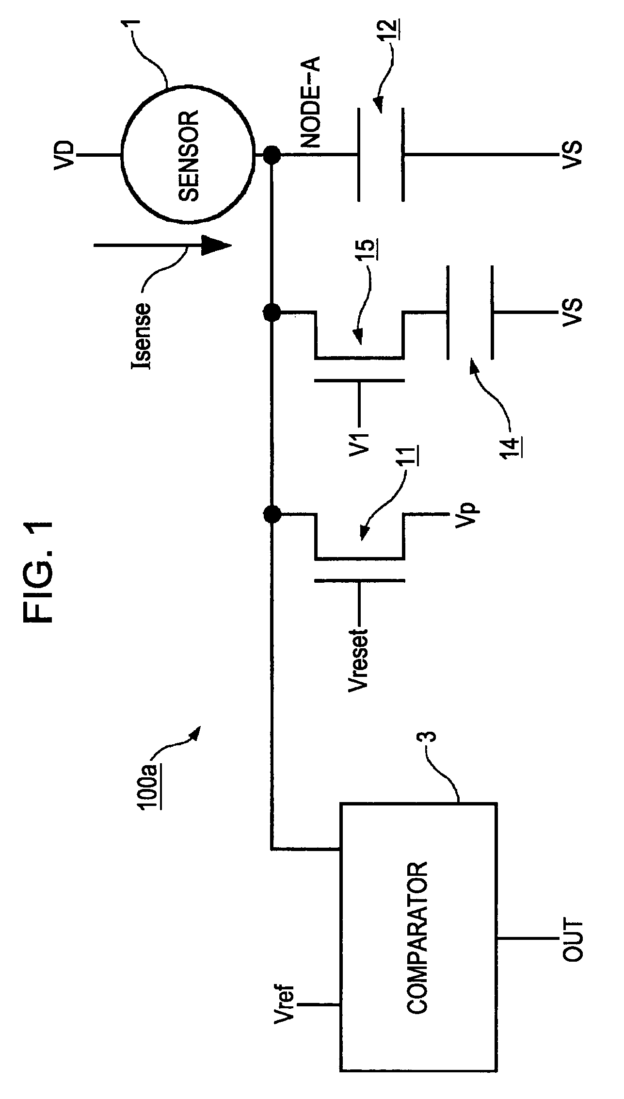
[0061]FIG. 1 is a diagram showing a sensor 1 and an A / D conversion circuit 100a realizing an electronic circuit in accordance with a first embodiment of the present invention. Elements that are the same as those of the known structure shown in FIG. 12 are designated by the same reference numerals, and a description thereof is omitted. In this circuit, a transistor is not used for conversion of the current Isense and the voltage VA, and a capacitor 12 serving as a first capacitive element and a capacitor 14 serving as a second capacitive element are placed. A transistor 15 serving as a range-switching circuit, a transistor 11 serving as a first switching element, and transistors constituting a comparator circuit 3 serving as a voltage detection circuit are field-effect transistors each including an active layer made of thin-film polysilicon disposed on a glass substrate serving as a substrate.

[0062]The capacitor 12, the capacitor 14, the transistor 15 and the transistor 11 constitute...

second embodiment

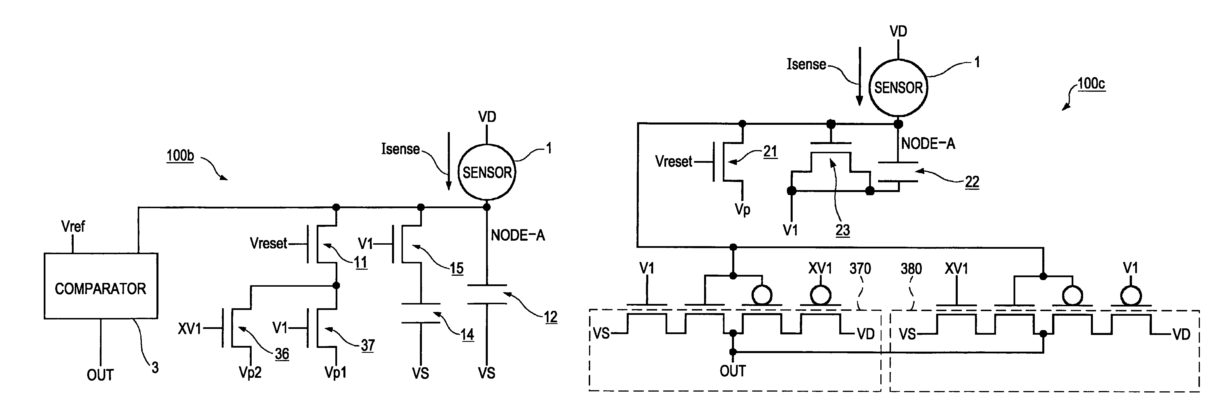
[0093]FIG. 9 is a circuit diagram showing a sensor 1 and an A / D conversion circuit 100b according to a second embodiment of the invention. A transistor 11 as a first switching element, a capacitor 12 as a first capacitive element, a capacitor 14 as a second capacitive element, and a transistor 15 as a range-switching circuit have the same structures and operate in the same manner as the elements represented by the same reference numerals in the first embodiment. The total capacitance C1 of the Node-A is 100 fF when V1=VS and 10 pF when V1=VD as in the first embodiment. The channel length and the channel width of each of transistors 36 and 37 are same as those of the transistor 15.

[0094]One end of the transistors 36 and 37 are connected via the transistor 11 to the Node-A, the other ends thereof are connected to voltages Vp2 and Vp1, respectively, thus constituting a reset voltage switching circuit that switches the reset voltage in response to a range-switching signal V1. A signal X...

third embodiment

[0098]FIG. 10 is a circuit diagram showing a sensor 1 and an A / D conversion circuit 100c according to a third embodiment of the invention. As a capacitance switching unit which is a range-switching circuit of the Node-A, instead of the structure including the capacitor and the switch shown in the first embodiment or the second embodiment, a field-effect capacitor in which source and drain electrodes of a transistor 23 are short-circuited with each other is used. The source and drain electrodes of the field-effect transistor 23 are connected to a range-switching signal V1. The voltage VA of the Node-A is between an initial voltage Vp and a reference voltage Vref, and VS+Vth23. A transistor 21 has a channel width W of 20 μm and a channel length L of 6 μm. The transistor 23 has a channel width W of 2,770 μm and a channel length L of 10 μm. A capacitor 22 has a capacitance of 100 fF.

[0099]When V1=VS, Vgs=Vp−VS>Vth, where Vgs is the voltage between the gate and the source of the transist...


PUM


Abstract

An electronic circuit, which has transistors disposed on a substrate, each transistor including an active layer made of thin-film polysilicon, includes a sensor that converts a measured quantity into a current value, a current-voltage conversion circuit that converts the current value into a voltage, and a voltage detection circuit that detects the voltage converted by the current-voltage conversion circuit and outputs a predetermined signal. The current-voltage conversion circuit includes a storage circuit and a range-switching circuit that switches a current-voltage conversion range of the current-voltage conversion circuit by switching the capacitance of the storage circuit.

Description

BACKGROUND[0001]1. Technical Field[0002]The present invention relates to electronic circuits, electro-optical devices, and electronic apparatuses including the same. More particularly, the invention relates to a circuit formed on a substrate using a thin-film polysilicon deposition technique, a liquid crystal display device including the circuit, and an electronic apparatus including the liquid crystal display device.[0003]2. Related Art[0004]In recent years, a technology in which various thin-film transistor circuits are formed on glass substrates using a low-temperature polysilicon deposition technique, i.e., a System On Glass (SOG) technology, has been actively developed. Examples include a monolithic driver in which a driver circuit is integrated onto a glass substrate of a liquid crystal display.[0005]As one application of the SOG technology, it is conceivable to form a sensor and its sensing circuit on a glass substrate. For example, by using a structure in which an optical se...

Claims


Application Information

Patent Timeline
Patent Type & Authority Patents(United States)
IPC IPC(8): G06F3/038
CPCG01J1/46G01J5/22H03M1/12G02F1/133
Inventor KOBASHI, YUTAKA
Owner JAPAN DISPLAY WEST
Why Eureka
Try Eureka