Method, apparatus and system for designing an integrated circuit including generating at least one auxiliary pattern for cell-based optical proximity correction

a technology of integrated circuits and auxiliary patterns, applied in the direction of program control, instrumentation, and semiconductor/solid-state device details, can solve the problems of large difference in feature critical dimensions between cell conventional and the runtime of model-based optical proximity correction tools, so as to reduce the runtime

Inactive Publication Date: 2011-01-18
RGT UNIV OF CALIFORNIA
View PDF2 Cites 169 Cited by
  • Summary
  • Abstract
  • Description
  • Claims
  • Application Information

AI Technical Summary

Benefits of technology

[0006]Methods and software of the invention also preferably make use of a methodology that inserts at least one vertical auxiliary pattern (“vertical-AP”) between horizontally adjacent cells, i.e., neighboring cells in the same cell row, so that cell-based optical proximity correction achieves the accuracy comparable to conventional model-based optical proximity correction methods with significantly reduced runtimes.

Problems solved by technology

However, the runtime of model-based optical proximity correction tools (i.e., software tools that use optical simulation and geometric operations to determine the photomask pattern for each layout feature) has grown unacceptably long with each successive technology generation, and has emerged as one of the major bottlenecks in the turnaround time for IC data preparation and manufacturing.
Unfortunately, optical proximity effects in lithography have a certain interaction radius between layout pattern geometries.
Since the neighboring environment of a cell in a full-chip layout is completely different from the environment of an isolated cell, the cell-based optical proximity correction solution can be incorrect when instantiated in a full-chip layout: as a result, there can be a large difference in feature critical dimensions between cell-based optical proximity correction and conventional model-based optical proximity correction.

Method used


Image

  • Method, apparatus and system for designing an integrated circuit including generating at least one auxiliary pattern for cell-based optical proximity correction
  • Method, apparatus and system for designing an integrated circuit including generating at least one auxiliary pattern for cell-based optical proximity correction
  • Method, apparatus and system for designing an integrated circuit including generating at least one auxiliary pattern for cell-based optical proximity correction

Examples


Embodiment Construction

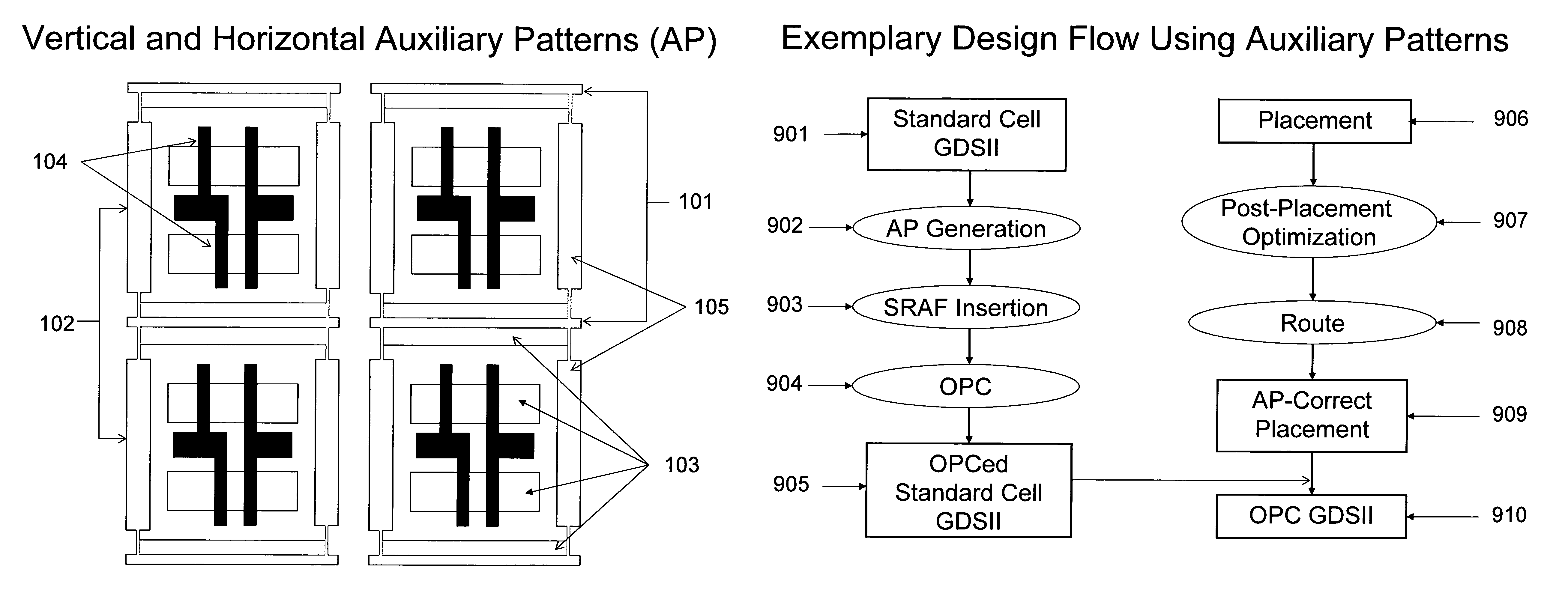
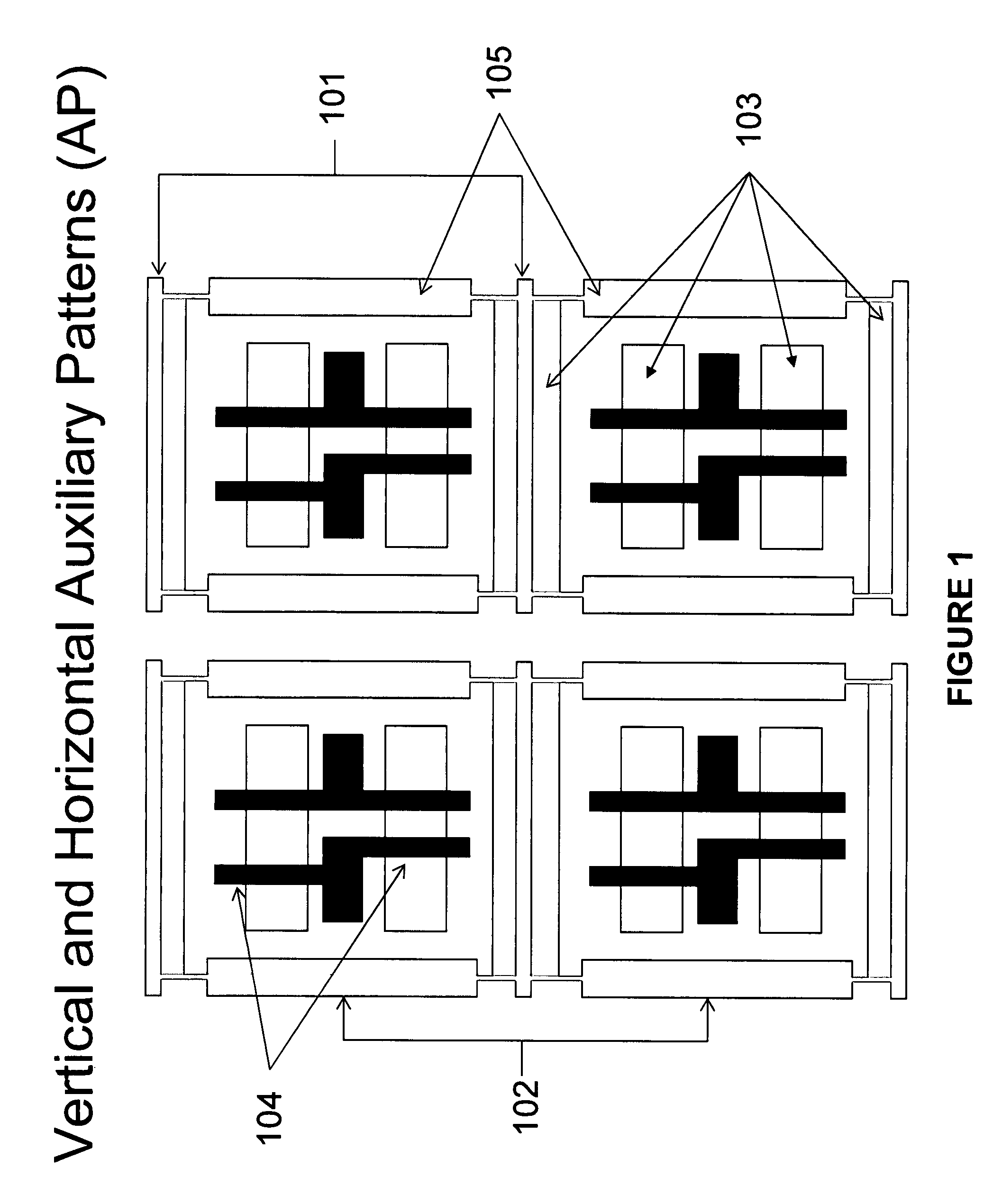
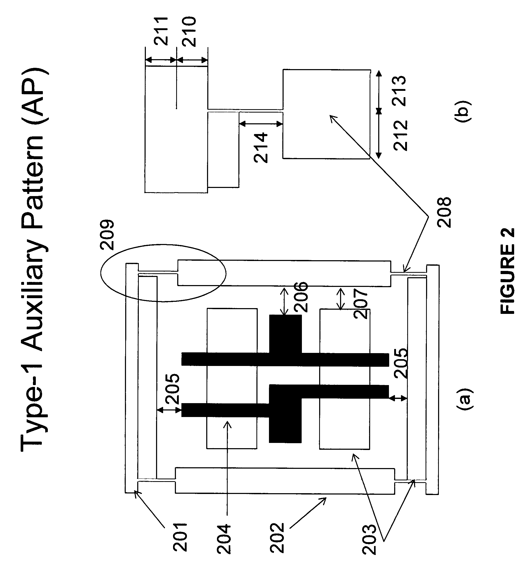
[0017]The invention provides systems and methods for auxiliary pattern generation for cell-based optical proximity correction. Embodiments of the invention provide software that uses methods to overcome deficiencies of prior cell-based optical proximity correction approaches by generating auxiliary patterns for a standard-cell layout and, optionally, performing a post-placement optimization of a standard-cell block to increase the number of auxiliary patterns (and hence the quality of cell-based optical proximity correction) in the overall block design. Software of the invention processes an existing standard-cell layout (e.g., input in GDSII Stream format) and then generates a new standard-cell GDSII which has added into it auxiliary patterns as well as subresolution assist features (the latter type of features are known as “scattering bars”, or SRAFs). Added auxiliary pattern features include vertical (V-AP) and / or horizontal (H-AP) auxiliary patterns. V-AP features print on the w...


PUM


Abstract

Method and apparatus for designing an integrated circuit. A new layout is generated for at least one standard cell that incorporates an auxiliary pattern on a gate layer to facilitate cell-based optical proximity correction. An original placement solution is modified for a plurality of standard cells to permit incorporation of cells containing auxiliary patterns while improving an objective function of a resulting placement solution for the plurality of standard cells.

Description

PRIORITY CLAIM AND REFERENCE TO RELATED APPLICATION[0001]This application claims priority under 35 U.S.C. §119 from prior related co-pending provisional application Ser. No. 60 / 837,575, which was filed on Aug. 14, 2006.FIELD[0002]Fields of the invention include integrated circuits and integrated circuit manufacturing.BACKGROUND[0003]Optical proximity correction (OPC) has been a key enabler of the aggressive IC technology scaling implicit in Moore's Law. Optical proximity correction determines the photomask patterns that enable drawn layout features to be faithfully and accurately reproduced by optical lithography onto a semiconductor wafer. However, the runtime of model-based optical proximity correction tools (i.e., software tools that use optical simulation and geometric operations to determine the photomask pattern for each layout feature) has grown unacceptably long with each successive technology generation, and has emerged as one of the major bottlenecks in the turnaround time...

Claims


Application Information

Patent Timeline
Patent Type & Authority Patents(United States)
IPC IPC(8): G06F17/50
CPCG06F17/5072G06F30/392
Inventor KAHNG, ANDREW B.PARK, CHUL-HONG
Owner RGT UNIV OF CALIFORNIA
Why Eureka
Try Eureka