Method to form a pattern of functional material on a substrate using a mask material

a technology of mask material and functional material, which is applied in the field of mask material for forming a functional material pattern on a substrate, can solve the problems of complex multi-step process, too costly for plastic electronics printing, and limited to forming metal patterns, microcontact printing of devices and components having patterns,

Inactive Publication Date: 2011-01-25
EI DU PONT DE NEMOURS & CO
View PDF27 Cites 16 Cited by
  • Summary
  • Abstract
  • Description
  • Claims
  • Application Information

AI Technical Summary

Benefits of technology

[0010]So it is desirable to provide a method for forming a pattern of a functional material, such as a conductor, semiconductor, or dielectric material, onto a substrate. It is also desirable for such method to have the ease of microcontact printing with an elastomeric stamp, but not be limited to printing onto metals. It is also desirable for such a method to avoid the problem of transfer of the functional material in featureless areas of the pattern.

Problems solved by technology

Photolithography, however, is a complex, multi-step process that is too costly for the printing of plastic electronics.
SAM printing is capable of creating high resolution patterns, but is generally limited to forming metal patterns of gold or silver with thiol chemistry.
However, microcontact printing of devices and components having the pattern of fine resolution lines of functional material separated by relatively large featureless areas where no functional material resides can be problematic.
Sagging of the relief surface can cause the recessed areas to print material where there should be no material.
If the material transferred is large, it may contact one or more of the pattern lines of the functional material, which can destroy the use of the component.
Microcontact printing of conductive patterns, particularly using SAM layers, where the sagging of the stamp transfers material onto background areas can lead to shorting the devices or components.
In addition to the feature density pattern incorporated in the stamp, the elastic nature of stamp may contribute to sagging in featureless areas.
However the features of the stamp may have an aspect ratio (determined by the width of features divided by height of features on the stamp) such that sagging is caused in the recessed areas between the pattern of fine resolution line features.

Method used


Image

  • Method to form a pattern of functional material on a substrate using a mask material
  • Method to form a pattern of functional material on a substrate using a mask material
  • Method to form a pattern of functional material on a substrate using a mask material

Examples


example 1

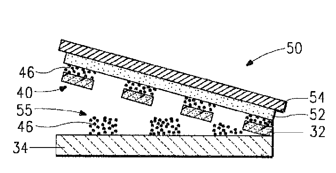
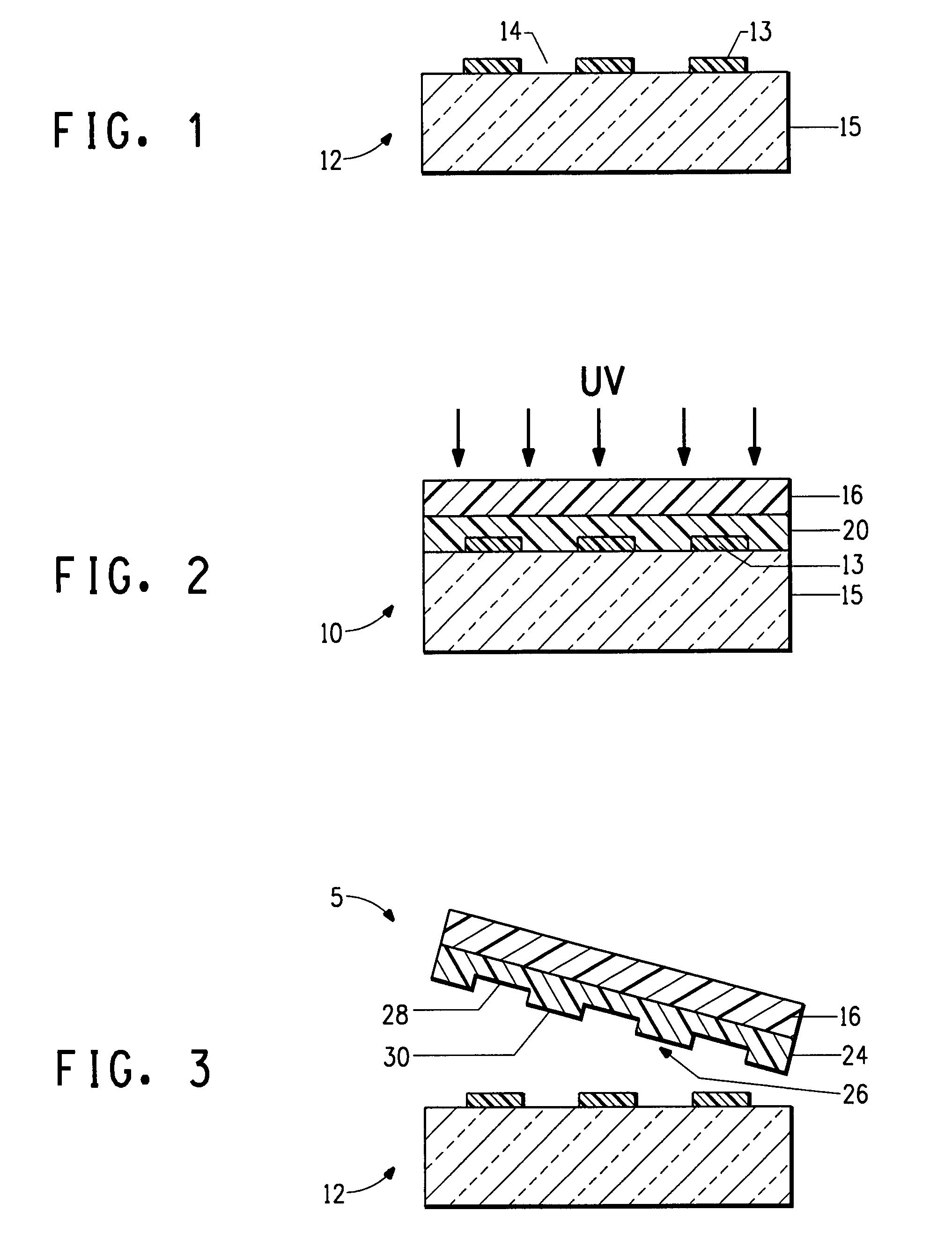
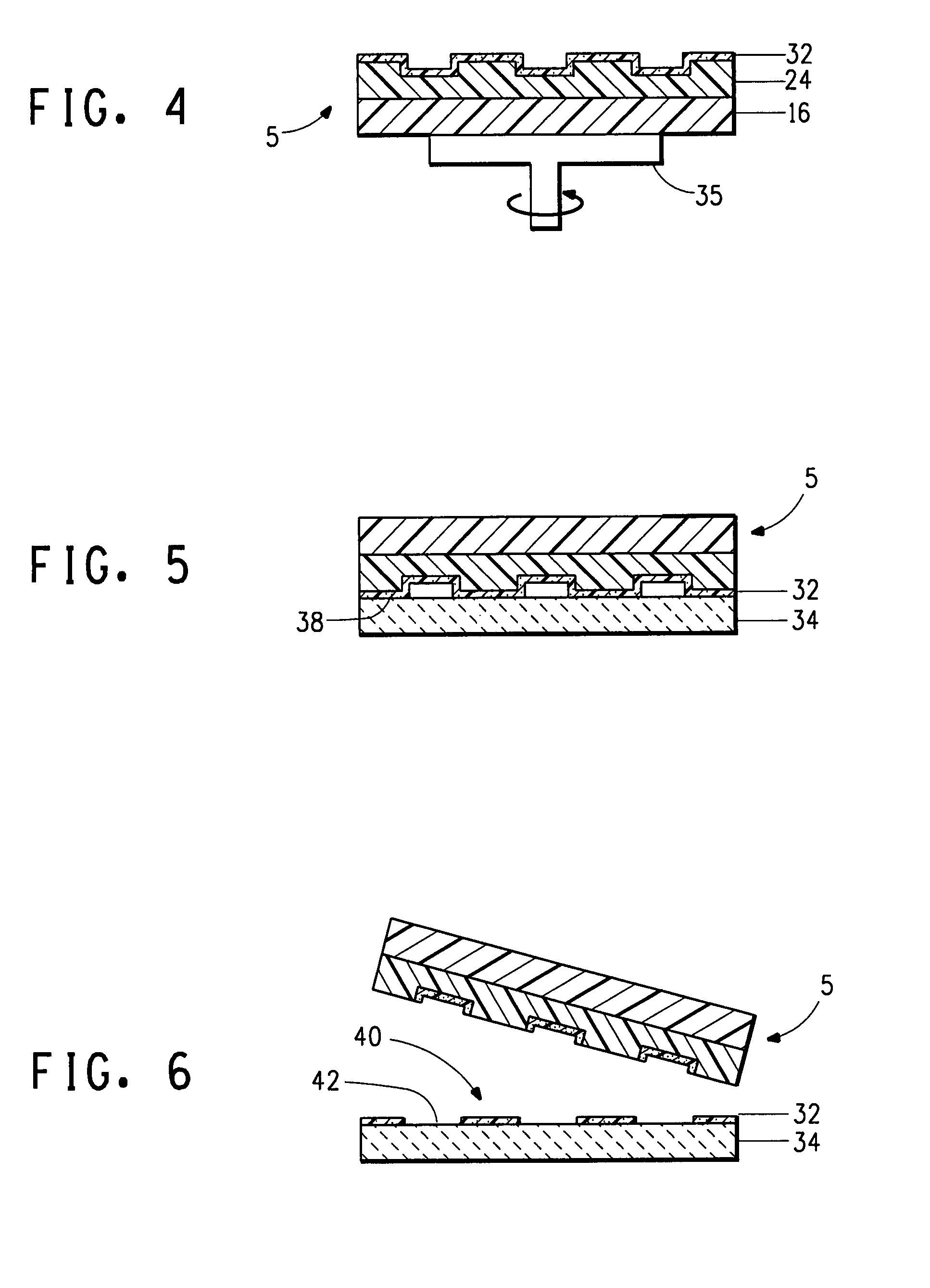
[0071]The following example demonstrates a method to form a pattern on a substrate using an elastomeric stamp to print a mask material. Silver nanoparticles were formed into a pattern onto a flexible base that can provide a functional source-drain level of a thin film transistor.

Master Preparation:

[0072]A thin hexamethyldisilazane layer (HMDS) (from Aldrich) was spun coated onto a 2 inch (5.1 cm) silicon wafer at 3000 rpm for 60 seconds. HMDS is an adhesion promoter for a photoresist material on a silicon wafer. A Shipley photoresist, type 1811 (from Rohm and Haas) was spun coated onto the HMDS layer at 3000 rpm for 60 seconds. The photoresist film was pre-baked on the hotplate at 115° C. for 1 minute to complete drying. The pre-baked photoresist film was then imagewise exposed to ultraviolet radiation of 365 nm for 8 seconds in an I-liner (OAI Mask Aligner, Model 200). After exposure the photoresist was developed in developer type MF-319 (from Rohm and Haas) that is tetramethyl amm...


PUM

PropertyMeasurementUnit
thicknessaaaaaaaaaa
thicknessaaaaaaaaaa
thicknessaaaaaaaaaa

Abstract

The invention provides a method to form a pattern of functional material on a substrate for use in electronic devices and components. The method uses a stamp having a relief structure to transfer a mask material to a substrate and form a pattern of open area on the substrate. The functional material is applied to the substrate in at least the open area. Contact of an adhesive material to an exterior surface opposite the substrate and separation of the adhesive from the substrate forms the pattern of functional material on the substrate. The method is suitable for the fabrication of microcircuitry for electronic devices and components.

Description

BACKGROUND OF THE INVENTION[0001]1. Field of the Invention[0002]This invention pertains to a method for forming a pattern of functional material on a substrate, and in particular, the method uses an elastomeric stamp having a relief surface to form a pattern of open area on the substrate where the functional material is applied.[0003]2. Description of Related Art[0004]Nearly all electronic and optical devices require patterning. Microelectronic devices have long been prepared by photolithographic processes to form the necessary patterns. According to this technique a thin film of conducting, insulating, or semiconducting material is deposited on a substrate and a negative or positive photoresist is coated onto the exposed surface of the material. The resist is then irradiated in a predetermined pattern, and irradiated or non-irradiated portions of the resist are washed from the surface to produce a predetermined pattern of resist on the surface. To form a pattern of a conducting met...

Claims


Application Information

Patent Timeline
Patent Type & Authority Patents(United States)
IPC IPC(8): B05D1/32
CPCB41M3/006B82Y10/00B82Y40/00G03F7/0002H01L51/0004H05K3/048H05K1/097H05K2203/0108H05K2203/0537H10K71/13B41F17/00B41M3/00B41M5/03B82Y30/00
Inventor BLANCHET, GRACIELA BEATRIZLEE, HEE HYUN
Owner EI DU PONT DE NEMOURS & CO
Why Eureka
Try Eureka