Method for connecting a die assembly to a substrate in an integrated circuit and a semiconductor device comprising a die assembly

a technology of integrated circuits and die assemblies, which is applied in the direction of semiconductor devices, semiconductor/solid-state device details, electrical apparatus, etc., can solve the problems of high assembly reject rate, failed connection, wire short circuit, etc., and achieve the effect of reducing waste of materials, cost saving and time saving

Inactive Publication Date: 2011-02-01
INFINEON TECH AG
View PDF11 Cites 4 Cited by
  • Summary
  • Abstract
  • Description
  • Claims
  • Application Information

AI Technical Summary

Benefits of technology

[0010]This method replaces conventional wire bonding processes. It is advantageous as it facilitates bonding and more particularly increases the efficiency in chip bonding procedures.
[0016]One or more embodiments of the present invention offer the advantage of reducing the waste of materials which, in conventional systems and methods, are due to items rejected because of failures in the wire bonding process; for example, the failure of the wires to stick on bond pads and wedges, damaged wires and bonding units where the wires are bonded to the wrong pads and therefore have to be discarded. Further advantages of one or more embodiments of the present invention are a cost saving due to the materials used, a time saving as the bonding is carried out in one step rather than bonding each wire separately, and much less skill is required from the operator when applying the methods embodying the invention than when using conventional processes. Also, the forming of complex wire loops such as the crossing of wires, high / low loops and the different modes of bonding does not occur due to the presence of the flexible strip.

Problems solved by technology

Poor settings of the process parameters and / or inappropriate wire and capillary selection may lead to a high assembly reject rate with associated problems like wire short circuits, neck ball, failed connections to the pads and / or leads, cratering of the pad and other problems.
Even with a single die device there is a problem in bonding the connections from the dies to the substrate and such problems are increased in multi-stack devices, particularly in wire bond / wire bond mode or flip-chip / wire bond mode.
In particular, the molding process can detach the wires or bring them into contact with adjacent wires causing short circuits.
Short circuiting may also be caused by wire strays, wire leaning and wire sweep after molding or wire bonding and can affect the performance of the device.
Conventional methods of electrically interconnecting the stacked die to the substrate have a number of defects.
In particular, conventional methods may suffer from one or more of the following problems, such as wire shorting due to die placement offset, inappropriate wire and capillary use, wrong parameter settings (wire loops), mishandling of bonded strips, excessive wire sweep after molding, non-stick-on pad due to the wrong parameter setting (USG current), contamination of the bond pad, large probe mark size and wrong bonding.
Furthermore, wire leaning and / or wire sways immediately after wire bonding could affect the performance of molding with the high possibility of wire shorting as a result.
In addition, inappropriate loop length and height of the loops, as well as weak interconnect adhesion could all further aggravate the encapsulation process.
Also, a capillary touching a wire and a wire touching the die edge could both result in poor bonding performance, which affects the operation of the device.

Method used


Image

  • Method for connecting a die assembly to a substrate in an integrated circuit and a semiconductor device comprising a die assembly
  • Method for connecting a die assembly to a substrate in an integrated circuit and a semiconductor device comprising a die assembly
  • Method for connecting a die assembly to a substrate in an integrated circuit and a semiconductor device comprising a die assembly

Examples


Embodiment Construction

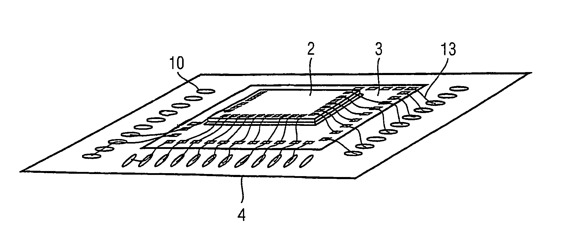
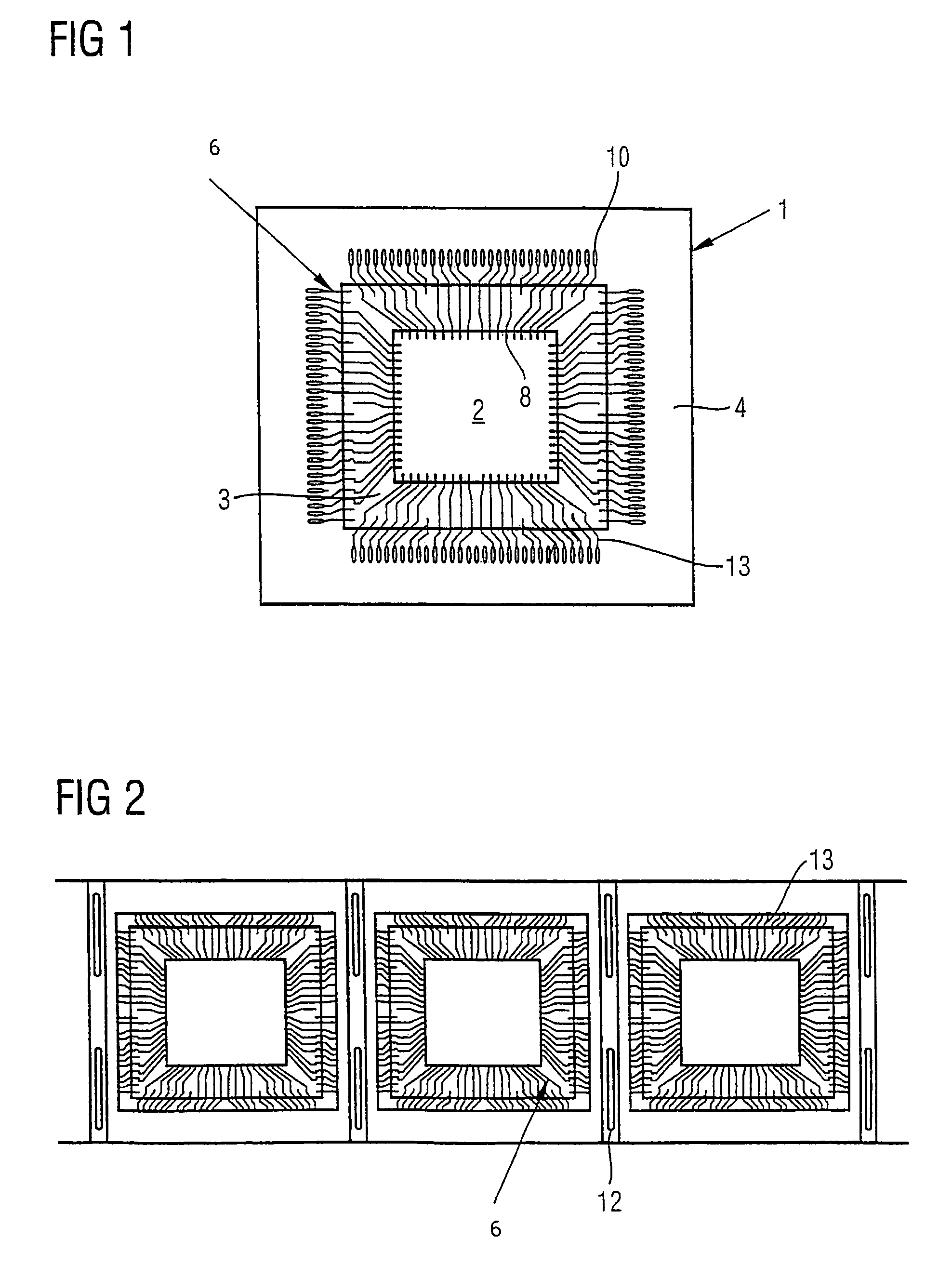
[0022]FIGS. 1 and 2 show a multi-die device 1 comprising two dies 2, 3, one die being mounted on top of the other, the top die 2 having a smaller surface area than the lower die 3. The pair of dies 2, 3 are mounted as a unit on a substrate 4. A plurality of flexible strips 6 are used to electrically connect the contacts 8 on the dies 2, 3 to each other (die-to-die) and the contacts 8 on the dies 2, 3 to the bond fingers 10 on the substrate 4. The flexible strips 6 may be formed of, for example, polyimide material.

[0023]The strips 6 may be manufactured in a variety of thicknesses depending upon the specifications of the bonding pitch. The length and width can be the same as the leadframe. The length and width of the polyimide strips are designed to be the same as the lead frame, having a conductive strip width of around between 0.75 to 1 μm.

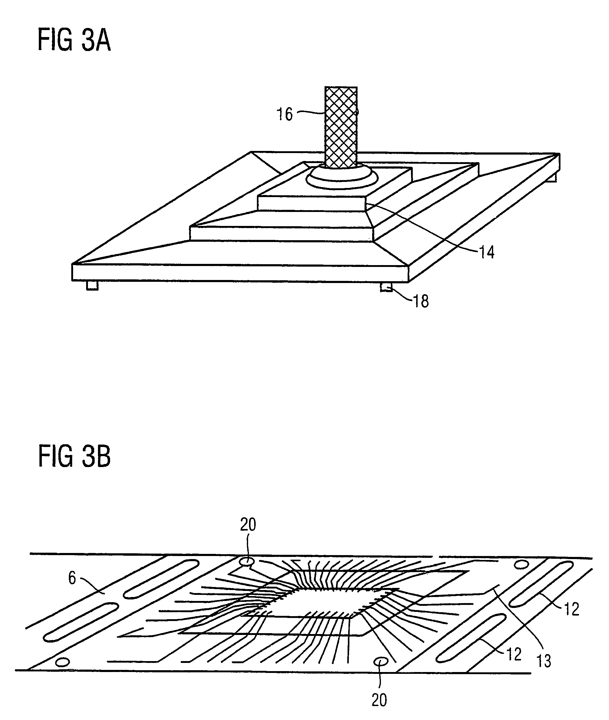
[0024]FIG. 2 shows a number of the flex strips 6. The strips 6 may have a number of location holes 12 for ease of positioning the strip 6 relativ...


PUM

PropertyMeasurementUnit
thicknessaaaaaaaaaa
thicknessaaaaaaaaaa
widthaaaaaaaaaa

Abstract

A semiconductor device includes a substrate, a die assembly attachable to the substrate and a flexible strip extending over the substrate and the die assembly. The flexible strip has one or more routing circuits carried thereon. The die assembly and the substrate are arranged to be electrically connected through the one or more routing circuits carried on the flexible strip.

Description

[0001]This application is a continuation of co-pending International Application No. PCT / SG2004 / 000011, filed Jan. 12, 2004, which designated the United States and was published in English, of which application is incorporated herein by reference.TECHNICAL FIELD[0002]The present invention relates to a method for connecting a die assembly to a substrate in an integrated circuit and a semiconductor device for use in an integrated circuit.BACKGROUND[0003]In conventional integrated circuits, particularly memory chips, several dies may be stacked on top of each other in a package to increase the overall capacity of the device. A ball grid array (BGA) structure is typically used for the stacked-die structure device. In such devices, a first semiconductor die is attached to the substrate via an adhesive layer. A wire bonding process is applied to electrically connect the first die to the substrate. A second die is then stacked on the first die with an adhesive layer formed between the firs...

Claims


Application Information

Patent Timeline
Patent Type & Authority Patents(United States)
IPC IPC(8): H01L23/495H01L21/60H01L21/603H01L21/607H01L21/98H01L23/538H01L25/065
CPCH01L23/49572H01L25/0657H01L25/50H01L24/86Y10T29/49162H01L2224/50H01L2224/86203H01L2224/86205H01L2225/06579H01L2924/01013H01L2924/01027H01L2924/01082H01L2924/14H01L24/48H01L2224/32145H01L2224/48145H01L2224/73265H01L2224/92247H01L2924/01033H01L2924/014Y10T29/49169Y10T29/49155H01L2924/00012H01L2924/00H01L2924/181H01L24/73H01L2924/00014H01L24/49H01L2224/05554H01L2224/49171H01L24/50H01L2224/45099H01L2224/45015H01L2924/207
Inventor SEAH, ALVINFERNANDEZ, ELSTAN ANTHONY
Owner INFINEON TECH AG
Why Eureka
Try Eureka