Display device

a display device and display technology, applied in the field of display devices, to achieve the effect of excellent electric characteristics, high reliability and high productivity

Inactive Publication Date: 2011-02-15
SEMICON ENERGY LAB CO LTD
View PDF7 Cites 16 Cited by
  • Summary
  • Abstract
  • Description
  • Claims
  • Application Information

AI Technical Summary

Benefits of technology

[0010]In view of above-mentioned problems, an object of the present invention is to offer a display device including an n-channel thin film transistor and a p-channel thin film transistor each having excellent electric characteristics and high reliability and a method for manufacturing the display device with high productivity.
[0013]Formation of a microcrystalline semiconductor film is hindered by oxygen. However, ultra high vacuum evacuation in a deposition chamber enables promotion of the formation of the microcrystalline semiconductor film because the oxygen concentration in the chamber can be reduced. In addition, oxygen results in a defect and functions as a donor in the microcrystalline semiconductor film. Therefore, particularly in the p-channel thin film transistor, the concentration of oxygen which functions as a donor can be reduced, thereby the mobility of the p-channel thin film transistor can be raised.
[0014]When a deposition temperature of the microcrystalline semiconductor film is set at 100 to 300° C., preferably 120 to 280° C., more preferably 120 to 220° C., lattice distortion at the interface between the gate insulating film and the microcrystalline semiconductor film can be reduced and characteristics of the interface between the gate insulating film and the microcrystalline semiconductor film can be improved. Therefore, electric characteristics of the thin film transistor having the microcrystalline semiconductor film can be improved.
[0016]One aspect of the present invention is a display device including a protective circuit on the periphery of a pixel portion, in which each of an inverted-staggered p-channel thin film transistor and an inverted-staggered n-channel thin film transistor is diode-connected. The protective circuit is provided between the pixel portion and a driver circuit, or over the opposite side of the driver circuit across the pixel portion, so that damages and deterioration due to static electricity can be prevented.
[0020]According to the present invention, a display device including an n-channel thin film transistor and a p-channel thin film transistor each having excellent electric characteristics and high reliability can be manufactured with high productivity.

Problems solved by technology

In addition, oxygen results in a defect and functions as a donor in the microcrystalline semiconductor film.

Method used


Image

  • Display device
  • Display device
  • Display device

Examples


embodiment mode 1

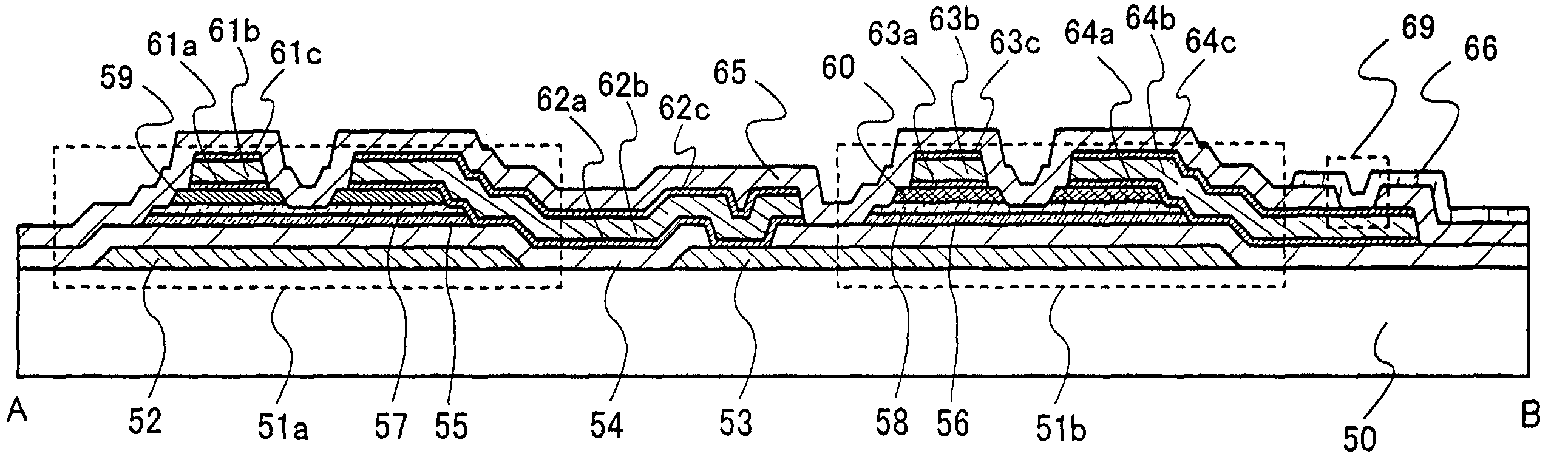
[0046]The structure of a pixel included in a display device of this embodiment mode is described. FIG. 1A illustrates one mode of the top plan view of a pixel. FIG. 1B illustrates one mode of the equivalent circuit diagram of a pixel. FIG. 1C illustrates one mode of the cross-sectional structure of a pixel along A-B in FIG. 1A.

[0047]In FIGS. 1A to 1C, a first thin film transistor 51a and a second thin film transistor 51b correspond to a switching thin film transistor for controlling input of a signal to a pixel electrode or a driving thin film transistor for controlling current or voltage application to a light-emitting element 68.

[0048]A gate electrode of the first thin film transistor 51a is connected to a scan line 52, one of a source or a drain of the first thin film transistor 51a is connected to wirings 61a to 61c which function as signal lines, and the other of the source or the drain is connected to a gate electrode 53 of the second thin film transistor 51b. One of a source ...

embodiment mode 2

[0082]In this embodiment mode, a plasma CVD apparatus and the method for depositing the gate insulating film, the microcrystalline semiconductor film, the buffer layer, the n-type semiconductor film, the p-type semiconductor film, the protective insulating film, and the like, which are described in Embodiment Mode 1, are described with reference to FIG. 3, FIG. 4, FIG. 5, and FIG. 24.

[0083]FIG. 3 illustrates one structure example of the plasma CVD apparatus to which high-frequency power is applied. A reaction chamber 400 is formed with a material having rigidity, such as aluminum or stainless steel, and provided with a system for performing vacuum evacuation inside the reaction chamber 400. The reaction chamber 400 is provided with a first electrode 401 and a second electrode 402.

[0084]The structure of the plasma CVD apparatus is such that the first electrode 401 is connected to a high-frequency power supply means 403, a ground potential is applied to the second electrode 402, and a...

embodiment mode 3

[0117]Next, light-emitting devices which are one mode of display devices are described with reference to FIGS. 1A to 1C, FIGS. 6A to 6C, and FIG. 7. As such light-emitting devices, light-emitting elements utilizing electroluminescence are used for description, here. Light emitting elements utilizing electroluminescence are classified according to whether a light-emitting material is an organic compound or an inorganic compound. In general, the former is referred to as an organic EL element and the latter is referred to as an inorganic EL element.

[0118]In the case of an organic EL element, by applying a voltage to the light-emitting element, electrons and holes are injected from a pair of electrodes into a layer containing an organic compound with a light-emitting property to cause a current flow. Then, recombination of these carriers (the electrons and holes) results in an excited state of the organic compound with a light-emitting property, and light is emitted when the excited sta...


PUM


Abstract

A display device including both an n-channel thin film transistor and a p-channel thin film transistor each having excellent electric characteristics and high reliability is demonstrated, and a method for manufacturing thereof is also provided. The display device includes an inverted-staggered p-channel thin film transistor and an inverted-staggered n-channel thin film transistor in which a gate insulating film, a microcrystalline semiconductor film, and an amorphous semiconductor film are sequentially stacked over a gate electrode. The microcrystalline semiconductor film contains oxygen at a concentration of 1×10¹⁶ atoms / cm3 or less. Mobilities of the n-channel thin film transistor and the p-channel thin film transistor are from 10 to 45 cm2 / V·s and 0.3 cm2 / V·s or less, respectively.

Description

BACKGROUND OF THE INVENTION[0001]1. Field of the Invention[0002]The present invention relates to a display device using an n-channel thin film transistor and a p-channel thin film transistor.[0003]2. Description of the Related Art[0004]In recent years, a technology to form thin film transistors using semiconductor thin films (with a thickness of approximately several tens to several hundreds of nanometers) that are formed over substrates having an insulating surface has attracted attention. Thin film transistors have been widely applied to electronic devices such as ICs and electro-optical devices and rapidly developed especially as switching elements for image display devices.[0005]A Thin film transistor using an amorphous silicon film for a channel formation region, a thin film transistor using a polycrystalline silicon film for a channel formation region, or the like are used as a switching element in an image display device. As a method for forming polycrystalline silicon films,...

Claims


Application Information

Patent Timeline
Patent Type & Authority Patents(United States)
IPC IPC(8): H01L29/04H01L21/336H01L21/822H01L21/8234H01L21/8238H01L27/04H01L27/06H01L27/08H01L27/092H01L29/786H01L51/50
CPCH01L27/1233H01L27/1288H01L29/04H01L29/78696H01L27/3262H01L29/41733H01L29/458H10K59/1213H01L27/092H01L27/1222
Inventor YAMAZAKI, SHUNPEIARAI, YASUYUKISUZUKI, YUKIEKUROKAWA, YOSHIYUKI
Owner SEMICON ENERGY LAB CO LTD
Why Eureka
Try Eureka