Light emitting device

a technology of light emitting device and light source, which is applied in the direction of discharge tube luminescnet screen, discharge tube/lamp details, electric discharge lamps, etc., can solve the problems of device inability to be used in continuous use applications, high manufacturing cost, and insufficient heat dissipation, etc., to achieve high reliability, thin and compact

Active Publication Date: 2011-02-15
NICHIA CORP
View PDF15 Cites 11 Cited by
  • Summary
  • Abstract
  • Description
  • Claims
  • Application Information

AI Technical Summary

Benefits of technology

[0010]It is an object of the present invention to provide a highly reliable light emitting device that is thin and compact, and a method for manufacturing this device.

Problems solved by technology

A light emitting device such as this is expensive to manufacture because it entails so many manufacturing steps and parts.
Furthermore, heat generated by the light emitting element is radiated to the outside through the substrate, which is composed of an insulating material with low thermal conductivity, so heat dissipation is inadequate.
As a result, when a high-output light emitting element is used, the device cannot be used in applications where continuous use is desirable.
The heat dissipation path can be shortened by making the insulating substrate thinner, but if this is done the electroconductive member formed on the upper face may not be strong enough.
Thus, it has been difficult to increase the heat dissipation of a light emitting device and at the same time keep the device thin and compact.
However, the side faces of the electrodes embedded in the resin are substantially parallel to the embedding direction, so impact and so forth encountered during mounting to a circuit board or during use after mounting can easily cause the electrodes to separate from the resin, resulting in a less integral structure in the light emitting device.
Particularly in the case of a light emitting device, since the insulating member that seals the light emitting element has to be made translucent, the mechanical strength cannot be increased by adding a filler or the like, making it extremely likely that this problem will occur.
Moreover, no specific method for manufacturing this light emitting device has been described.

Method used


Image

  • Light emitting device
  • Light emitting device
  • Light emitting device

Examples


example 1

[0049]Using strip-shaped SUS 430 with a thickness of 60 μm as the metal matrix material, an intermediate layer composed of titanium was formed on the upper face of this metal matrix material, and this product was heat treated in a hydrogen gas atmosphere.

[0050]Next, a resist was formed in a thickness of 70 μm, and the resist was patterned so that an opening measuring 0.5×0.2 mm and an opening measuring 0.5×1.0 mm were arranged in parallel at a pitch of 0.2 mm.

[0051]A gold / nickel layer was formed in the openings. The upper face of the nickel layer was formed lower than the upper face of the resist. The gold layer was then formed so as to be higher than the resist upper face. The gold layer (the topmost layer) was then silver plated.

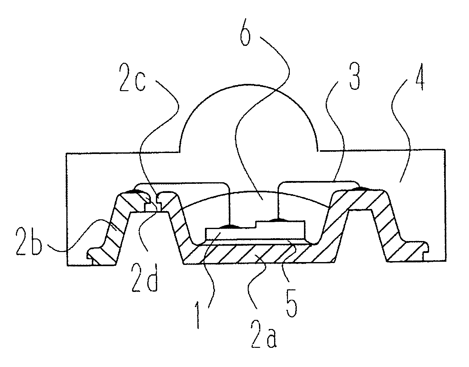
[0052]Finally, the resist was removed to obtain electroconductive layers 2a and 2b having protrusions 2c and 2d with a thickness and protruding length of 50 μm each.

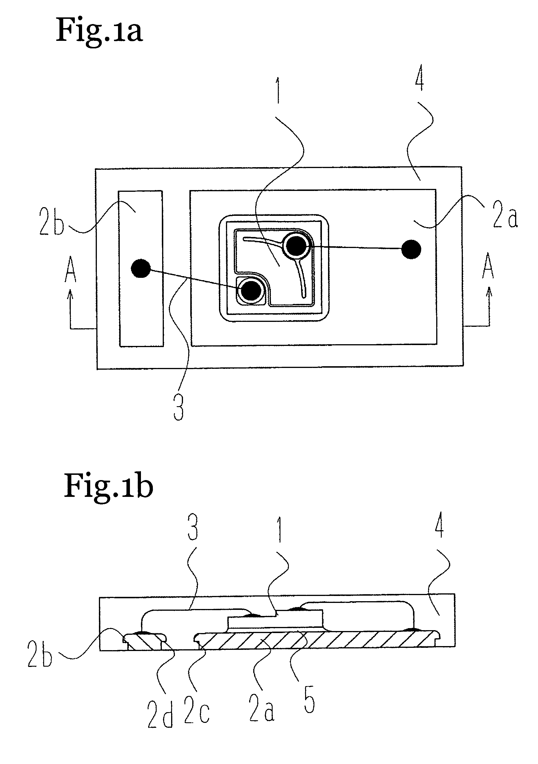
[0053]Then, a light emitting element 1 was electrically connected to the pair of electrocon...

example 2

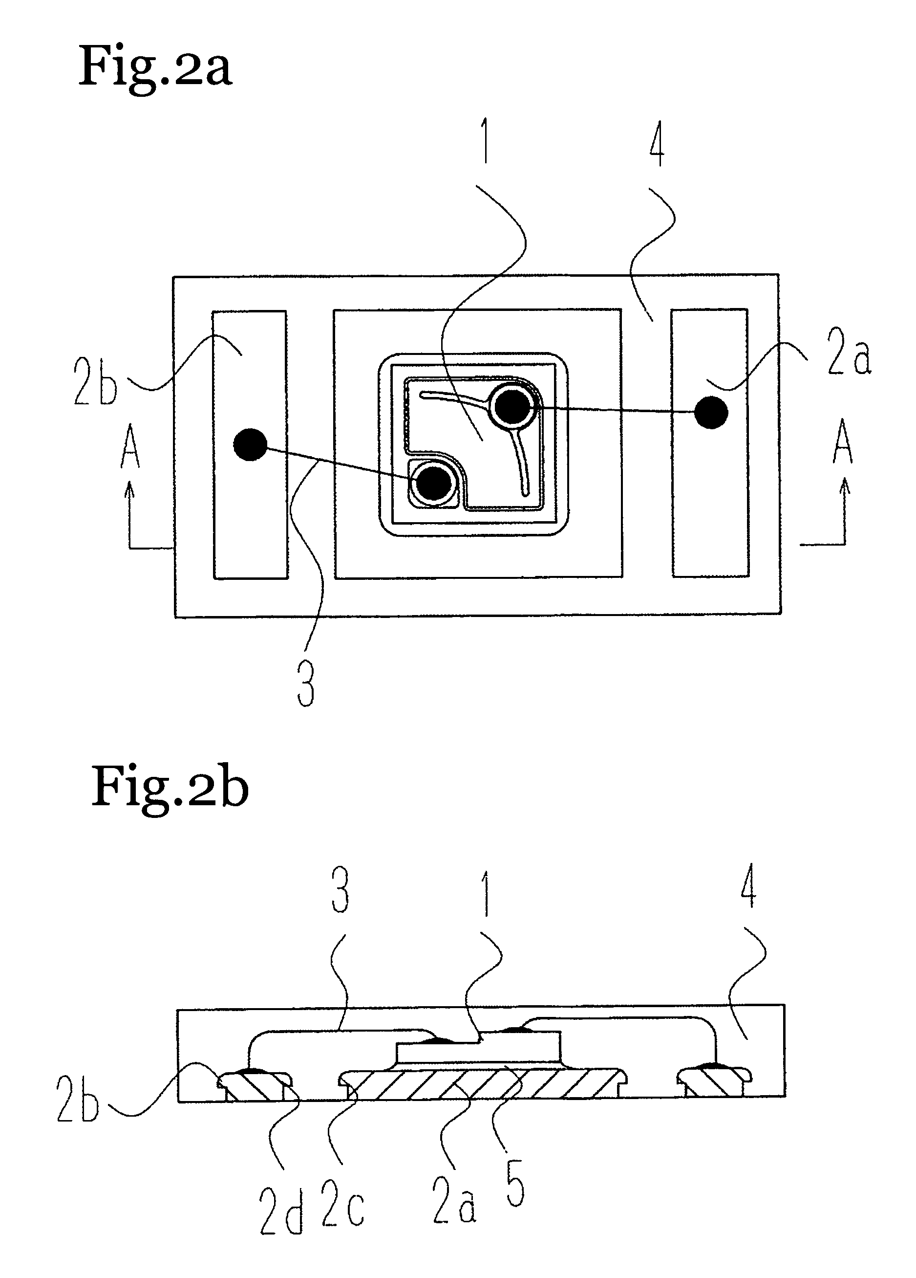
[0058]The light emitting device shown in FIGS. 2a and 2b was obtained in the same manner as in Example 1, except that the resist was patterned so that an opening measuring 0.5×0.2 mm, an opening measuring 0.5×1.0 mm, and an opening measuring 0.5×0.2 mm were arranged in parallel at a pitch of 0.2 mm, there were two electroconductive layers for wire bonding in one light emitting device, and there was one electroconductive layer for holding the light emitting element. The light emitting device obtained in this manner had better heat dissipation than the one in FIGS. 1a and 1b.

example 3

[0059]A plurality of recesses were formed to a depth of 80 μm by etching ahead of time in the metal matrix material, and an electroconductive layer 2a equipped with a recess capable of holding a light emitting element 1 was formed.

[0060]Next, the light emitting element 1 was placed in the above-mentioned recess, and the electrodes of the light emitting element 1 were electrically connected by wires 3 to the electroconductive layers 2a and 2b, after which the recess was filled with a color conversion member 6 containing a fluorescent substance capable of absorbing light from the light emitting element and converting it to a longer wavelength. More specifically, a silicone resin and a (Y0.8Gd0.2)3Al5O12:Ce0.03 fluorescent substance were mixed in a weight ratio of 100:15 with stirring, and the recess was filled with the resulting mixture and left for 4 hours, allowing the fluorescent substance to settle. The fill amount is preferably enough to produce a shape that will protrude in the ...


PUM


Abstract

A light emitting device, comprises a light emitting element, a plurality of electroconductive layers on which said light emitting element is mounted or which are electrically connected to the light emitting element, and a translucent insulating member that seals the light emitting element and has the electroconductive layers as its bottom surface, wherein the electroconductive layers have a protrusion on part of their side faces, and the upper edges of the protrusion is rounded off.

Description

BACKGROUND OF THE INVENTION[0001]1. Field of the Invention[0002]The present invention relates to a light emitting device, and more particularly relates to a light emitting device that is used in lighting, automobiles, industrial devices, and consumer devices (such as displays), and can be used to advantage in thin and compact surface mounting applications, and to a method for manufacturing this light emitting device.[0003]2. Background Information[0004]An example of a conventional surface mount type of light emitting device is a light emitting device in which a light emitting element is electrically connected to a pair of electroconductive members formed in a pattern on the surface of an insulating substrate made of glass epoxy, ceramic, or the like, and the area near the light emitting element is sealed with a translucent insulating member.[0005]A light emitting device such as this is expensive to manufacture because it entails so many manufacturing steps and parts. Furthermore, he...

Claims


Application Information

Patent Timeline
Patent Type & Authority Patents(United States)
IPC IPC(8): H01J1/62H01L33/50H01L33/54H01L33/32H01L33/56H01L33/62
CPCH01L33/486H01L33/62H01L2224/16H01L2224/48247H01L2924/0102H01L2924/01025H01L2924/01322H01L2924/01079H01L2924/09701H01L2924/10157H01L2924/19041H01L2924/3011H01L2924/01078H01L2924/181H01L2224/0603H01L2224/16245H01L2224/48091H01L2224/32245H01L2224/48257H01L2224/73265H01L2924/00014H01L2924/00012H01L33/52H01L33/48
Inventor TANDA, YUICHIROTAMAKI, HIROTO
Owner NICHIA CORP
Why Eureka
Try Eureka