Illuminating device, electro-optic device, and electronic apparatus

a technology of electrooptic devices and electronic devices, applied in the field of illumination devices, can solve the problems of low reliability, low luminous energy of led used as the light source in known portable backlights, and inability to meet the requirements of high brightness, so as to enhance the reliability of light sources and improve insulation and heat radiation

Inactive Publication Date: 2008-05-15
JAPAN DISPLAY WEST
View PDF9 Cites 22 Cited by
  • Summary
  • Abstract
  • Description
  • Claims
  • Application Information

AI Technical Summary

Benefits of technology

[0015]An advantage of some aspects of the invention is that it provides an illuminating device and other devices having a light source, which generates heat, mounted on a flexible substrate with a heat radiation route from the light source to a metal frame, optimized to enhance the insulation and the heat radiation and thus enhance the reliability of the light source.

Problems solved by technology

In particular, vehicle-mounted backlights are larger than portable backlights and require high brightness.
However, the LED used as the light source in known portable backlights has low luminous energy and inferior in reliability.
Such an LED is not suitable as the light source of the vehicle-mounted backlight.
Unfortunately, as the making current is increased, the junction temperature of the LED is increased.
Consequently the characteristics of the LED are varied and the reliability is degraded.
However, the above-mentioned Japanese Unexamined Patent Application Publication No. 2004-186004 disclosing an illuminating device and Japanese Registered Utility Model No. 3098463 disclosing a heat radiator for backlight-including LCDs do not describe the heat radiation route from the heat source, or the LED light source, and they do not necessarily provide optimal heat radiation structures.
Although Japanese Unexamined Patent Application Publication No. 2005-283852 disclosing a liquid crystal display device and Japanese Unexamined Patent Application Publication No. 2002-162626 disclosing a heat radiator of a light source for liquid crystal display describe the heat radiation route from the LED light source, the insulation between the mounting substrate and the metal case or between the film substrate and the frame is not taken into account sufficiently and is not ensured accordingly.
In particular, the liquid crystal display device of Japanese Unexamined Patent Application Publication No. 2005-283852 has a complicated heat radiation structure in, for example, the mounting substrate and is accordingly difficult to mass-produce.
Therefore, if the areas of the mounting metal film and the metal film pattern are increased from the viewpoint of heat radiation, it becomes difficult to route the driving metal wire and the conductivity is degraded.
If the driving metal wire is routed while the areas of the mounting metal film and the metal film pattern are increased, the width of the mounting substrate is disadvantageously increased.
In contrast, if the areas of the mounting metal film and the metal film pattern are reduced for ease of wire routing, the heat radiation performance is undesirably degraded.
Also, since the supported surface of the substrate is in close contact with the substrate-supporting surface of the first frame, heat conducted to the supported surface of the substrate can be further conducted to the frame without reducing the heat radiation efficiency.

Method used


Image

  • Illuminating device, electro-optic device, and electronic apparatus
  • Illuminating device, electro-optic device, and electronic apparatus
  • Illuminating device, electro-optic device, and electronic apparatus

Examples


modification 1

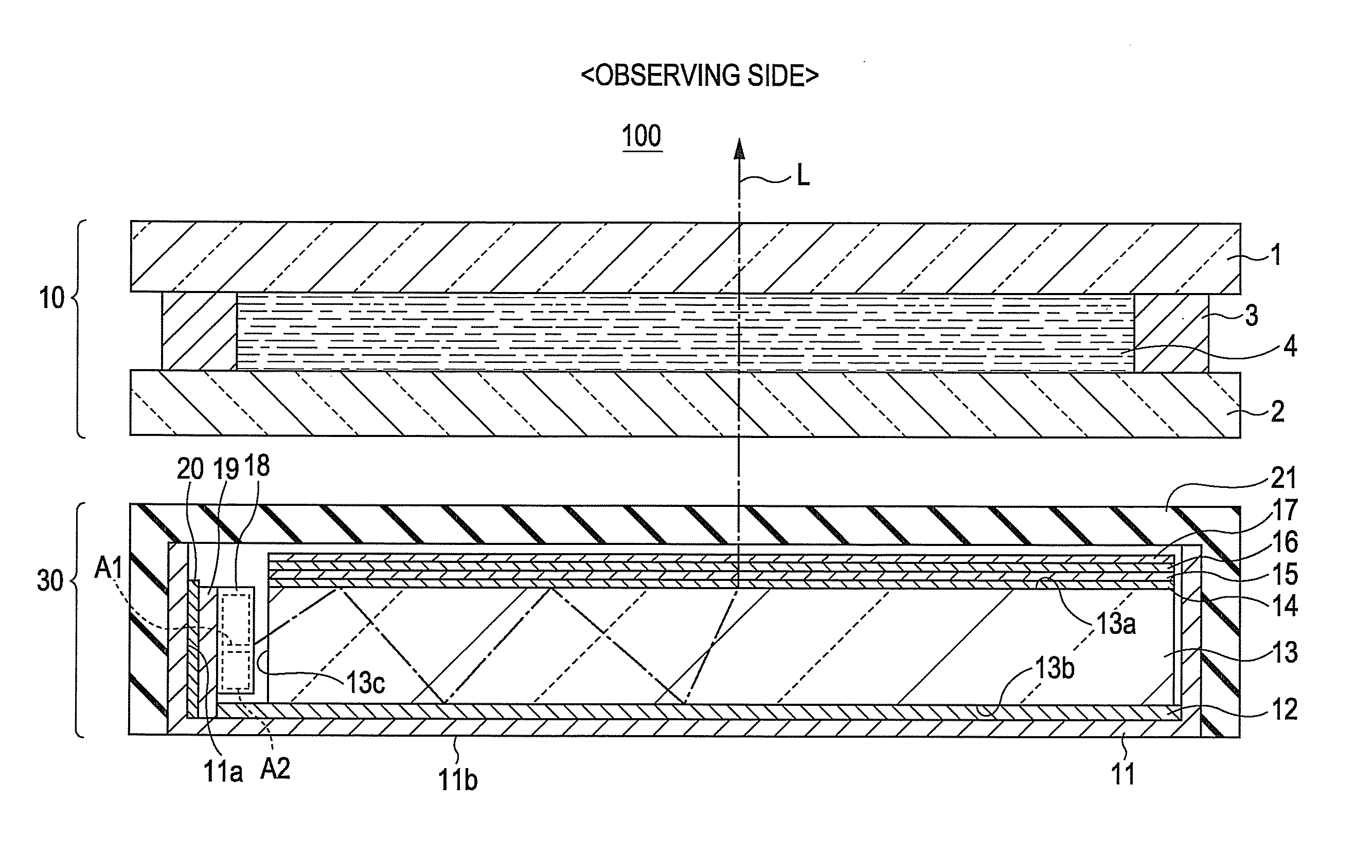
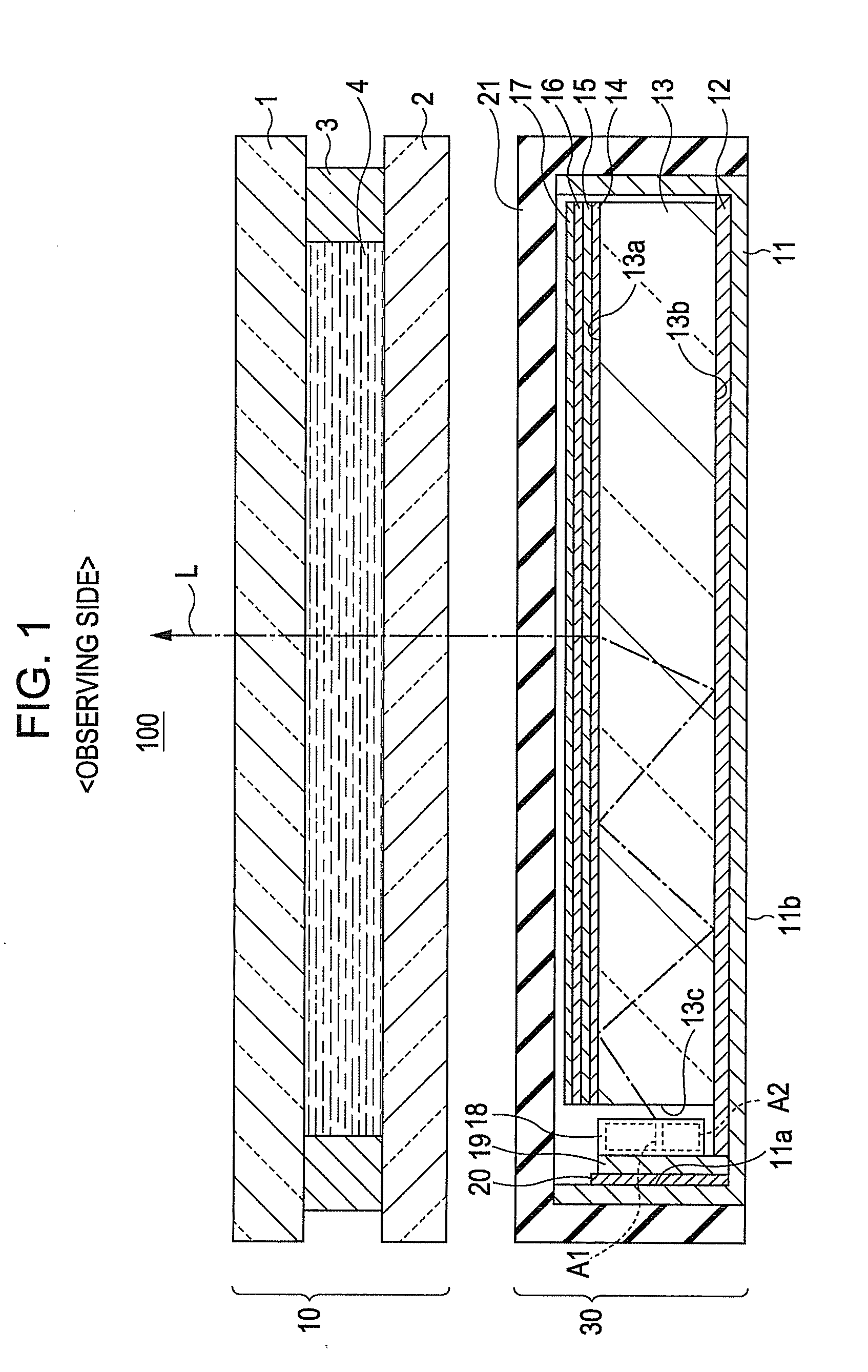
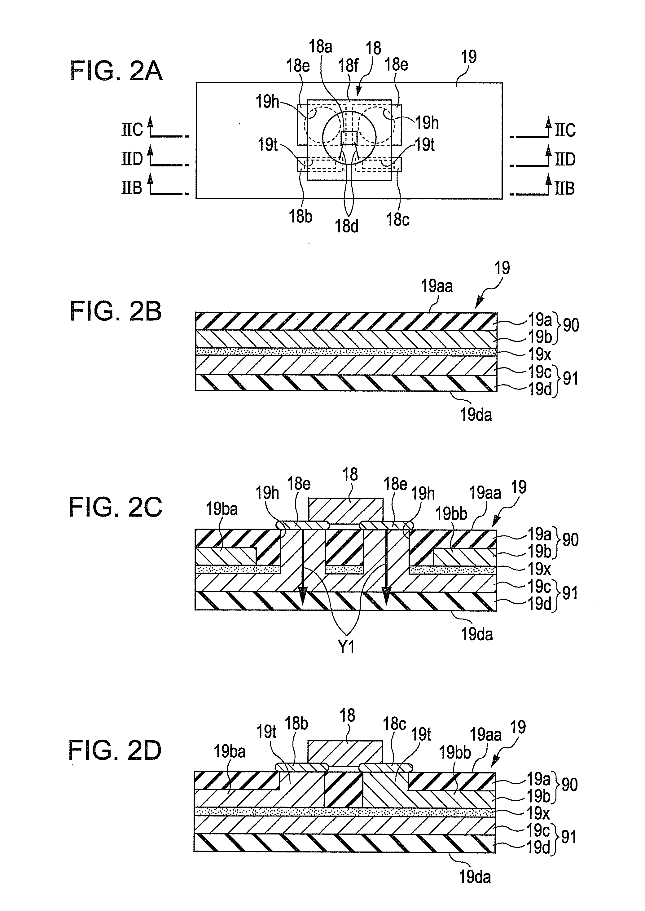
[0089]The flexible substrate 19 in the above-described embodiment has the insulative adhesive layer 19x between the first metal layer 19b and the second metal layer 19c. In addition to the adhesive layer 19x, an insulating layer similar to the first insulating layer 19a or the second insulating layer 19d may be disposed between the first metal layer 19b and the second metal layer 19c.

modification 2

[0090]The illuminating device 30 of the invention does not necessarily require the heat-conductive adhesive tape 20. The supported surface 19da of the second insulating layer 19d may be in direct close contact with the substrate-supporting surface 11a, as shown in FIG. 3B.

modification 3

[0091]The flexible substrate 19 may not have the second insulating layer 19d that is in contact with one surface of the electrically isolated second metal layer 19c. More specifically, this surface 19ca of the second metal layer 19c acts as the supported surface so as to be in contact with the substrate-supporting surface 11a of the first frame 11 with the heat-conductive adhesive tape 20 in between, as shown in FIG. 4A.


PUM


Abstract

An illuminating device includes a light source including a light-emitting element, an electrode electrically connected to the light-emitting element, and a heat radiation terminal electrically isolated from the light-emitting element; and a multilayer substrate including a plurality of insulating layers, a plurality of metal layers, an electrically conducting interlayer contact portion, and a heat-conducting interlayer contact portion. The insulating layers include all insulating layer having a mount surface on which the light source is mounted with the electrode and the heat radiation terminal therebetween. The metal layers include an electrically conducting metal layer electrically connected to the electrode and disposed so as to be separated from the light source by the insulating layer having the mount surface and an electrically isolated metal layer electrically isolated from the other metal layers and disposed most distant from the mount surface of all the metal layers. The electrically conducting interlayer contact portion electrically connects the electrode to the electrically conducting metal layer. The heat-conducting interlayer contact portion connects the heat radiation terminal to the electrically isolated metal layer.

Description

[0001]The entire disclosure of Japanese Patent Application Nos. 2006-307537, filed Nov. 14, 2006 and 2007-146545, filed Jun. 1, 2007 are expressly incorporated by reference herein.BACKGROUND[0002]1. Technical Field[0003]The present invention relates to an illuminating device suitably used in electro-optic devices.[0004]2. Related Art[0005]Liquid crystal devices, which are a type of electro-optic device, have a backlight at the rear side of the liquid crystal display panel for transmissively displaying images. In general, the backlight is a illuminating device including a light source, such as an LED (light emitting diode), and an optical waveguide allowing the rear surface of the liquid crystal display panel to be irradiated two-dimensionally with light emitted from the light source. A main type of backlight has a light source at an end surface of the optical waveguide and is, thus, called “edge light type”.[0006]In particular, vehicle-mounted backlights are larger than portable bac...

Claims


Application Information

Patent Timeline
IPC IPC(8): G02F1/1335F21V29/00H01K1/58
CPCG02B6/005G02B6/0083G02B6/0085G02F2001/133628H05K1/0206H05K2201/10106H05K1/0393H05K1/189H05K3/0061H05K2201/09309H05K1/0207G02F1/133628
Inventor SAKAI, TOYOHIRO
Owner JAPAN DISPLAY WEST
Why Eureka
Try Eureka