Statistical delay and noise calculation considering cell and interconnect variations

a technology of interconnection variation and delay, applied in the field of integrated circuit design performance analysis and optimization, can solve the problems of significantly affecting circuit performance and product yield, logic cell delay models are becoming more and more complicated, and methods are very time-consuming, and achieve low cost, high accuracy, and efficient calculation of nominal delay and its sensitivity over different parameters.

Active Publication Date: 2011-02-15
SYNOPSYS INC
View PDF5 Cites 159 Cited by
  • Summary
  • Abstract
  • Description
  • Claims
  • Application Information

AI Technical Summary

Benefits of technology

[0016]The invention provides a sensitivity-based statistical delay calculation methodology. The inventive method provides accurate nominal delay together with the delay sensitivities with respect to different circuit elements (e.g., cells, interconnects, etc.) and variational parameters such as fabrication process and environmental variations. The invention provides a statistical delay calculation methodology, which can efficiently calculate nominal delay and its sensitivity over different parameters. In the inventive statistical effective capacitance approach, all the sensitivity computations are based on closed-form formulas; consequently, the inventive method provides, rapidly and at low cost, high accuracy and high numerical stability.
[0017]The invention also provides a method for calculating waveform-based statistical noise and cross-talk delay. By means of “built-in” noise waveform alignment techniques, the method can accurately calculate statistical noise waveform and its impact on delay. The invention taught herein applies statistical Max and Sum operations to statistical noise waveform and noise envelope calculations.

Problems solved by technology

The transistor-level simulation method can accurately simulate the circuit timing behavior, but this method is very time-consuming and is not feasible for a full-chip analysis.
In static timing analysis, logic cell delay models are becoming more and more complicated as semiconductor technologies evolve.
These variations introduce uncertainty in circuit behaviors and significantly impact the circuit performance and product yield.
The increased variability has given a new set of problems for circuit timing analysis.
However, current delay calculation methods do not handle process and environmental variations from both cells and interconnects.
The corner-based methodology for worst-case analysis traditionally used in static timing analysis may be overly pessimistic as well as extremely inaccurate.
However, both path based and block based approaches focus not on delay calculation but on high level timing propagation problems wherein the delay is assumed (based on a simple model) rather than calculated.
Consequently, all nominal delay calculation approaches (such as, for example, the effective capacitance method) are not currently able to capture statistical information accurately.
Crosstalk between nanoscale size features also complicates statistical timing analysis.
Consequently, the delay of a gate can be greatly impacted by the switching activity on neighboring wires (see R. Arunachalam, K. Rajagopal and L. Pileggi, TACO: Timing Analysis with Coupling” Proceedings of the Design Automation Conference, pp.
The effects of crosstalk (“crosstalk effect”) pose two major problems.
In the case where the victim net is quiet (non-switching), capacitive crosstalk can induce noise (glitches) and potentially cause functional failures.
For example, if a glitch happens when the clock signal of a register is switching, the data in the register may be flipped accidentally.
If the aggressor is switching in the opposite direction, crosstalk can lead to an increase in delay, which may cause “setup time violations.” If the aggressor is switching in the same direction as the victim, crosstalk may lead to the delay decreasing, and may cause “hold time violations.”

Method used


Image

  • Statistical delay and noise calculation considering cell and interconnect variations
  • Statistical delay and noise calculation considering cell and interconnect variations
  • Statistical delay and noise calculation considering cell and interconnect variations

Examples


Embodiment Construction

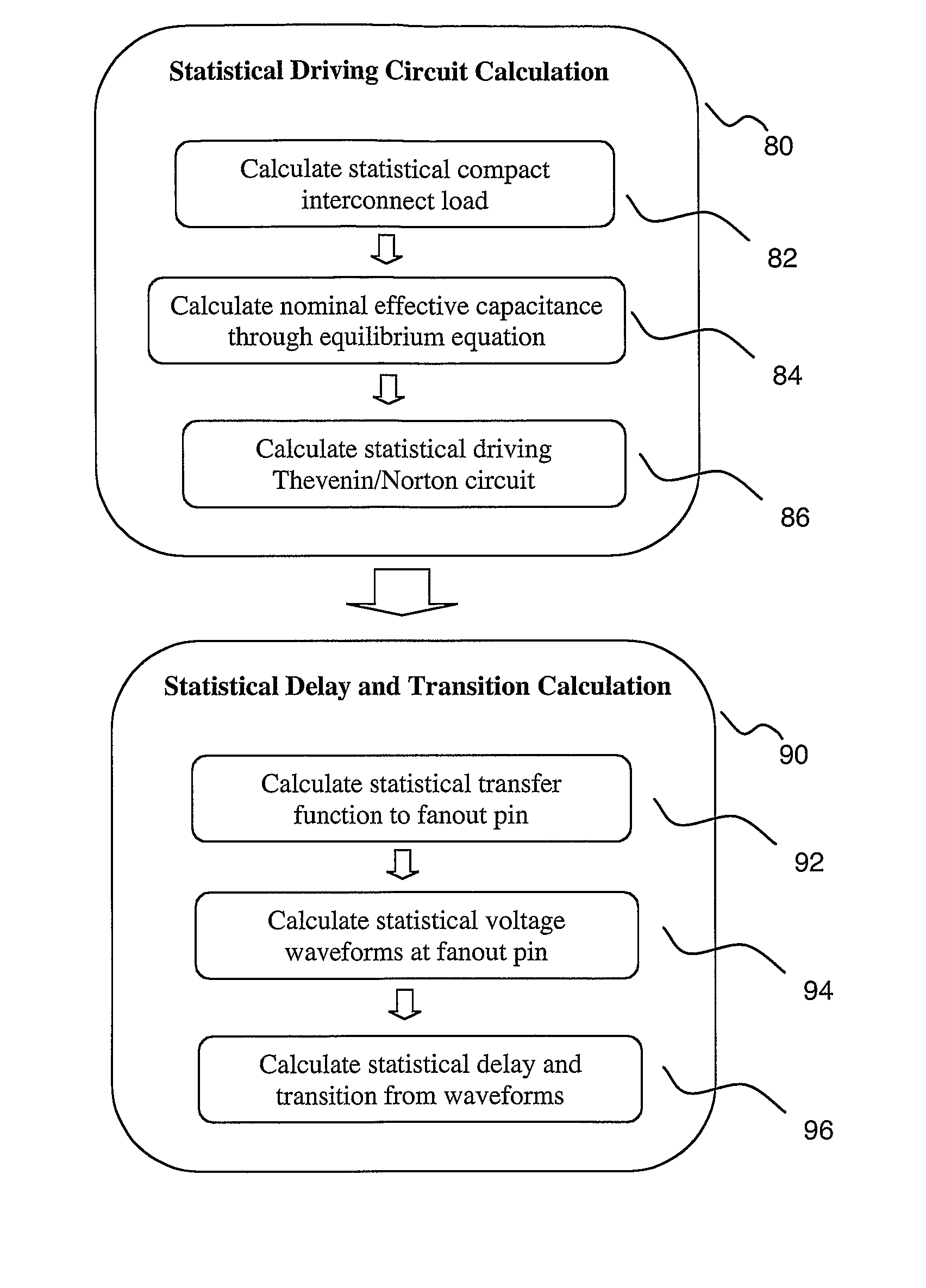
[0033]The invention taught herein is broadly represented in FIG. 1. The invention provides a method of determining statistical delay 302 considering non-linear input waveform and receiver capacitance. The invention further provides a method for statistical noise calculation 304 considering non-linear victim driver resistance model and multiple timing windows. The invention further provides statistical crosstalk delay calculation 306 combining non-cross-talk statistical delay and statistical noise information using pure analytical approaches and guarantee pessimism (i.e., satisfying a verification condition ensuring the IC chip circuits function).

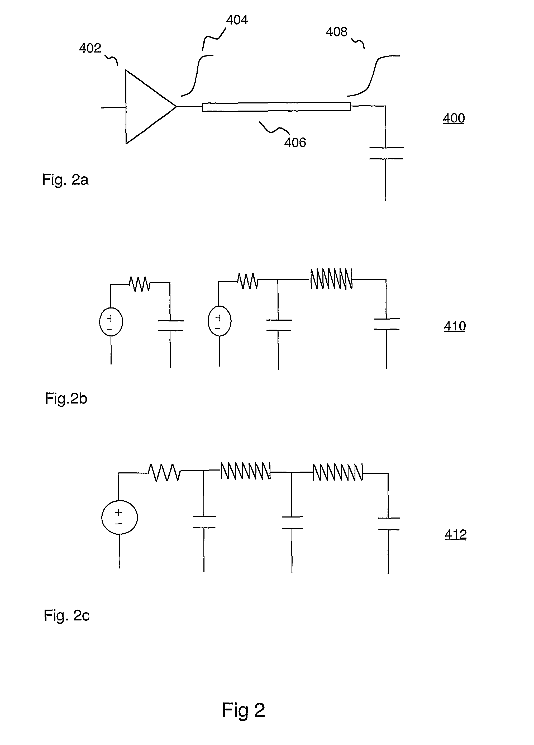
[0034]In modern VLSI digital circuit, logical cell delay is a function of different physical sources. Cell delay is a function of non-linear input waveform, non-linear receiver load capacitances, resistive interconnect load, crosstalk effect and process and environmental variations.

[0035]With the increasing effects of interconnect resistance...


PUM


Abstract

The electrical circuit timing method provides accurate nominal delay together with the delay sensitivities with respect to different circuit elements {e.g., cells, interconnects, etc.) and variational parameters (e.g., process variations; environmental variations). All the sensitivity computations are based on closed-form formulas; as a consequence, the method provides rapidly and at low cost high accuracy and high numerical stability.

Description

RELATED APPLICATIONS[0001]This application claims priority from U.S. provisional application 60 / 663,219, filed Mar. 18, 2005, and the contents of which are incorporated in their entirety as if fully set forth herein.GOVERNMENT FUNDING[0002]Not applicable.BACKGROUND[0003]1. Field of the Invention[0004]The invention generally relates to the field of integrated circuit design performance analysis and optimization, and particularly to the delay and crosstalk noise calculation for logic cells used in statistical static timing analysis of digital integrated circuit.[0005]2. Description of the Related Art[0006]In modern very large-scale integrated circuit (VLSI) design, it is very important to improve the circuit operating speed and to verify if the circuit can perform at a target frequency. To achieve these goals, circuit designers extensively use timing verification and optimization software from Electronic Design Automation (EDA) vendors on their designs. Two main methodologies for timi...

Claims


Application Information

Patent Timeline
Patent Type & Authority Patents(United States)
IPC IPC(8): G06F9/455G06F17/50
CPCG06F17/5031G06F30/3312
Inventor CELIK, MUSTAFALE, JIAYONG
Owner SYNOPSYS INC
Why Eureka
Try Eureka