Method for fabricating semiconductor device

a semiconductor device and manufacturing method technology, applied in the direction of semiconductor devices, basic electric elements, electrical appliances, etc., can solve the problems of increasing the number of steps, limiting the step of fabricating a semiconductor device having a minute line width equal or less than 60 nm, and affecting the use of pvd tungsten

Active Publication Date: 2011-03-01
SK HYNIX INC
View PDF22 Cites 0 Cited by
  • Summary
  • Abstract
  • Description
  • Claims
  • Application Information

AI Technical Summary

Benefits of technology

[0014]To solve the problem, the invention provides a method of fabricating a semiconductor device in which a tensile stress on an etched layer or an amorphous carbon film can be reduced in forming an amorphous carbon film, or a compression stress film is formed between the etched layer and the amorphous carbon film and thus a lifting phenomenon can be prevented from occurring.
[0017]A method of forming a semiconductor device according to another embodiment of the present invention may comprise the steps of forming an etched layer having a tensile stress on a semiconductor substrate, depositing an amorphous carbon film on the etched layer, and performing a heat treatment to eliminate the tensile stress on the etched layer.
[0020]A method of forming a semiconductor device according to another embodiment of the invention may include the steps of forming an etched layer on a semiconductor substrate, forming a compression stress film having a predetermined compression stress on the etched layer, and depositing an amorphous carbon film on the compression stress film, wherein the tensile stress on the amorphous carbon film can be reduced due to the compression stress on the compression film.

Problems solved by technology

Therefore, several problems arise in fabricating semiconductor devices forming a cell and various solutions has been tried to solve the aforementioned problems.
However, there is a limitation to the step of fabricating a semiconductor device having a minute line width equal to or less than 60 nm.
However, when the reflection preventing film and the hard mask are formed using a amorphous carbon film, a problem arises in that a lifting phenomenon occurs, which does not occur in forming the reflection preventing film and the hard mask using SiON and SiN.
However, since a burial step of a metal contact is difficult when a PVD tungsten film is used, in order to perform a step of using a PVD tungsten film, a prior CVD tungsten film is buried to form a metal contact and then a metal wire is formed using PVD tungsten.
Accordingly, the numbers of steps increase to become complicate in using PVD tungsten.

Method used


Image

  • Method for fabricating semiconductor device
  • Method for fabricating semiconductor device
  • Method for fabricating semiconductor device

Examples


embodiment 1

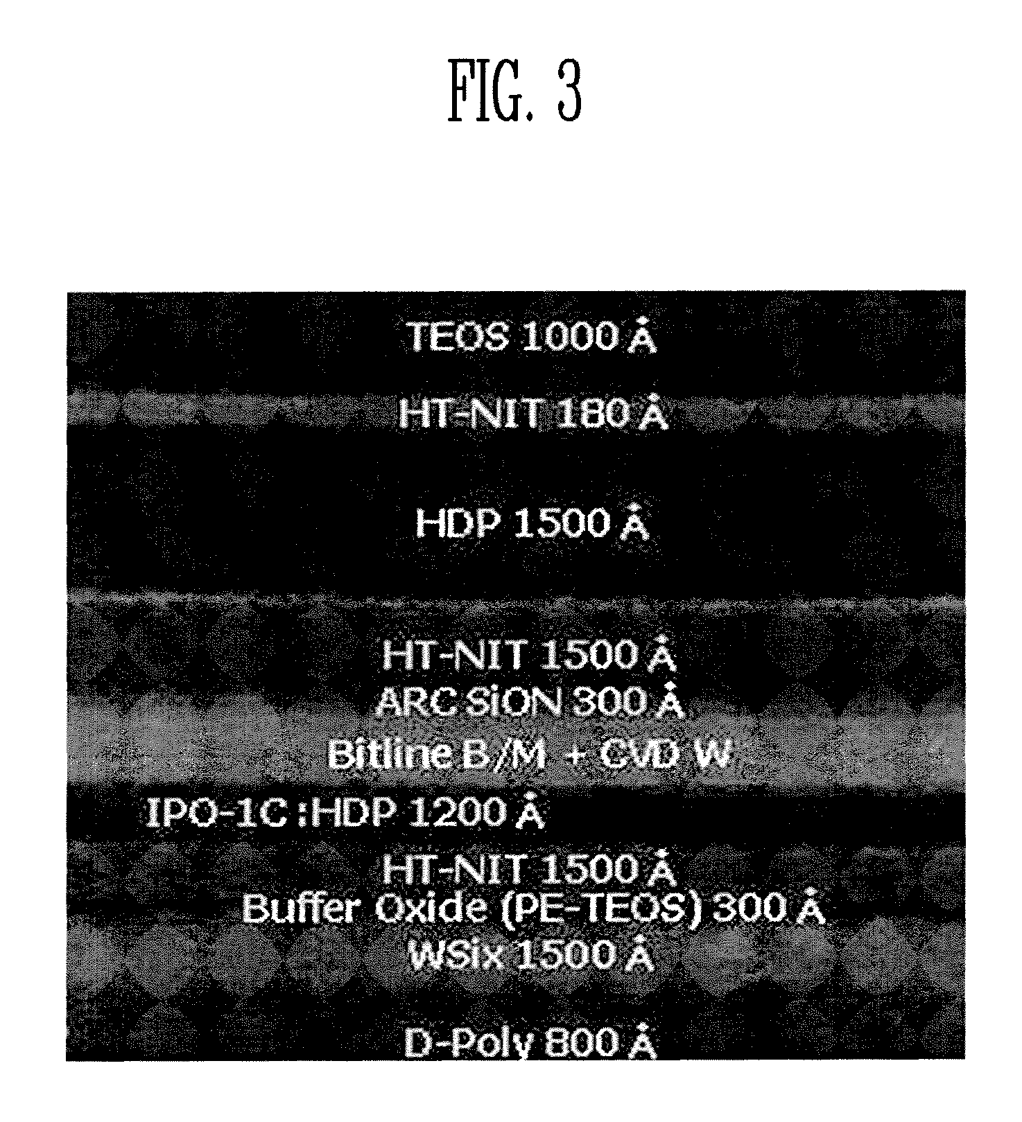
[0034]An amorphous carbon film having a compression stress is formed. Typically, the amorphous carbon film has a tensile stress of about 90 MPa at a forming temperature of 550° C. Here, when the amorphous carbon film is formed at below this temperature, preferably, 100° C.-400° C., the amorphous carbon film has a compression stress. For example, the amorphous carbon film is formed at 300° C., it has a tensile stress of about 330 MPa.

[0035]Accordingly, when an amorphous carbon film is formed over the etched layer, the amorphous carbon film is formed at a range of 100° C. to 400° C. and thus a lifting phenomenon on a stacked layer can be prevented. The following Table 3 shows stresses and stress concentration factors on a CVD tungsten film and an amorphous carbon film formed at 300° C., respectively, and a stress concentration factor on stacked layers formed by stacking them.

[0036]

TABLE 3FilmThickness (Å)Stress (dyn / cm2)Kc (MPa / m0.5)Amorphous carbon2000−3.30e+09−0.215filmCVD tungsten ...

embodiment 2

[0038]To reduce a tensile stress on an etched layer, a heat treatment process against the etched layer is performed. The heat treatment process for reducing a tensile stress on the etched layer is performed under an argon atmosphere at 300° C. to 500° C. for 0.5 hours to two hours, or under argon atmosphere at 300° C.-500° C. for one minute to 20 minutes through a Rapid Thermal Annealing process.

embodiment 3

[0039]A film having a compression stress is formed between a stacked layer of an etched layer and an amorphous carbon film. The film having a compression stress includes a Plasma Enhanced nitride film, an oxide film, SiON film and a strontium oxide film (SrOx), etc. The following Table 4 shows stresses and stress concentration factors on a CVD tungsten film, an amorphous carbon film, and a PE nitride film respectively, and a stress concentration factor on stacked layers formed by stacking the PE nitride film between the CVD tungsten film and the amorphous carbon film.

[0040]

TABLE 4FilmThickness (Å)Stress (dyn / cm2)Kc (MPa / m0.5)Amorphous carbon20009.00e+080.059filmPE nitride film300−2.60+09−0.066CVD tungsten film800 1.5e+100.619Total Kc on the Stacked layer0.338

[0041]Referring to Table 4, the stress concentration factor on the stacked layer is 0.038 MPa / m0.5, and thus a lifting phenomenon does not occur.

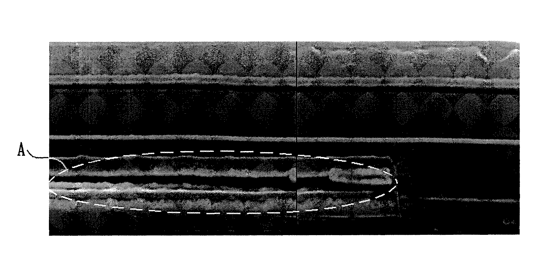
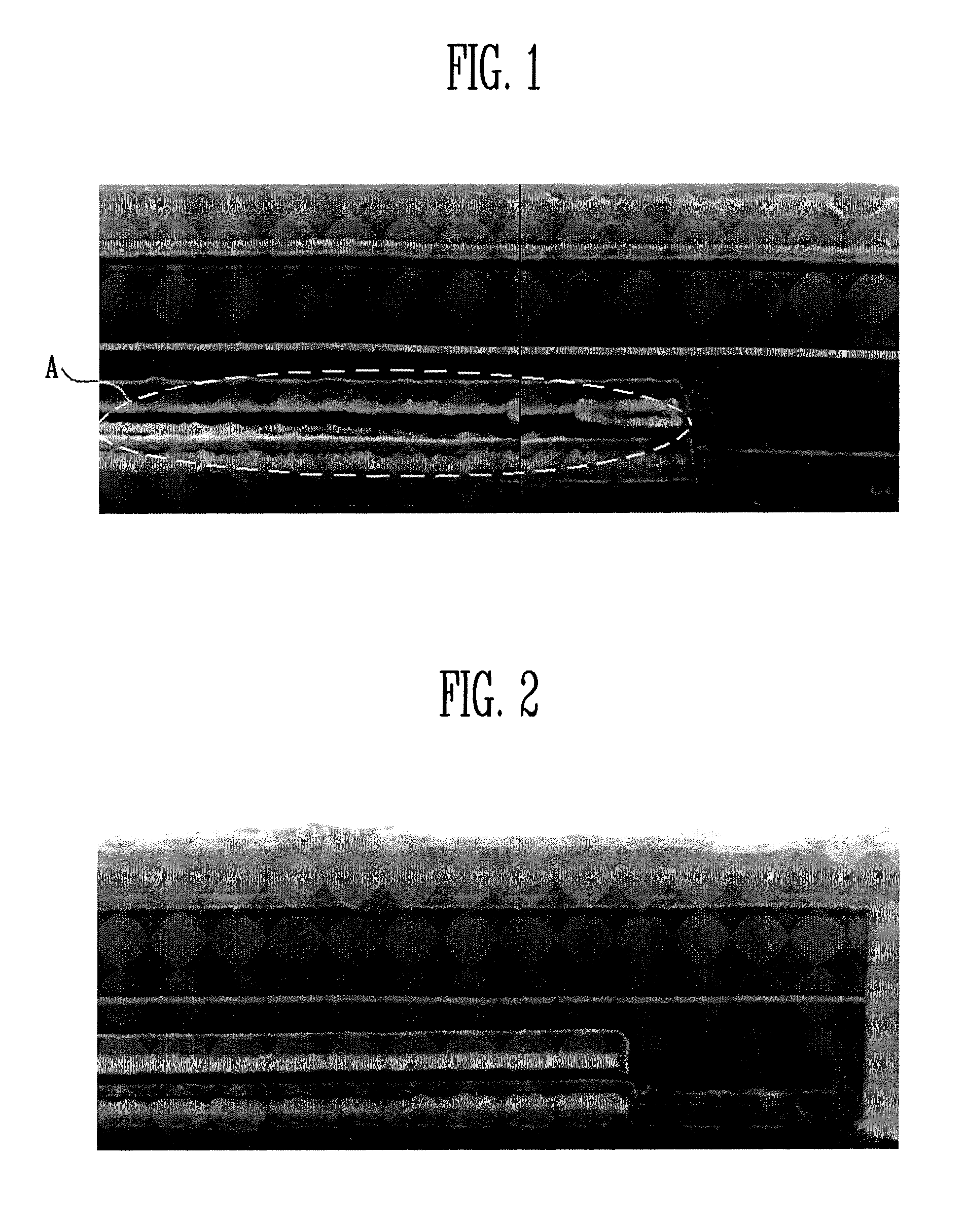
[0042]According to the method for fabricating a semiconductor device of the inventi...


PUM

PropertyMeasurementUnit
widthaaaaaaaaaa
widthaaaaaaaaaa
tensile stressesaaaaaaaaaa

Abstract

A method for fabricating a semiconductor device, in which a lifting phenomenon can be prevented from occurring in forming an amorphous carbon film on an etched layer having tensile stress. According to the invention, since a compression stress on the etched layer or the amorphous carbon film can be reduced or a compression stress film is formed between the etched layer or the amorphous carbon film to prevent a lifting phenomenon from occurring and thus another pattern can be formed to fabricate a highly integrated semiconductor device.

Description

CROSS-REFERENCE TO RELATED APPLICATION[0001]The priority of Korean patent application number 10-2006-96199, filed on Sep. 29, 2006, the disclosure of which is incorporated by reference in its entirety, is claimed.BACKGROUND OF THE INVENTION[0002]The invention relates to a method for fabricating a semiconductor device and, more particularly, to a method for fabricating a semiconductor device in which a lifting phenomenon can be prevented from occurring in forming an amorphous carbon film on an etched layer having tensile stress.[0003]As semiconductor devices have become more highly integrated, the devices have to be formed in a high density on a predetermined cell area and therefore unit devices such as a transistors and capacitors, etc. decrease in size. In particular, as a design rule decreases in a memory device such as a flash memory, semiconductor devices that are formed inside cells decrease generally in size. Recently, a minimum line width of a flash memory device is formed eq...

Claims


Application Information

Patent Timeline
Patent Type & Authority Patents(United States)
IPC IPC(8): H01L21/4763
CPCH01L21/0276H01L21/32139H01L21/28273H01L29/40114H01L21/306
Inventor KIM, JUNG GEUNJEONG, CHEOL MOCHO, WHEE WONMYUNG, SEONG HWAN
Owner SK HYNIX INC
Why Eureka
Try Eureka