Leakage current mitigation in a semiconductor device

a technology of leakage current and semiconductor devices, applied in the field of semiconductor devices, can solve the problems of leakage current runaway, mosfet devices, and leakage current, and achieve the effect of reducing current leakag

Inactive Publication Date: 2011-03-22
GLOBALFOUNDRIES INC
View PDF12 Cites 13 Cited by
  • Summary
  • Abstract
  • Description
  • Claims
  • Application Information

AI Technical Summary

Benefits of technology

[0009]a repair voltage generator which outputs a repair voltage to the aforesaid first switch control logic device, the aforesaid repair voltage being applied from the aforesaid first switch control logic device to the gate of the target semiconductor device in response to the aforesaid alert signal from the aforesaid comparator, the aforesaid alert signal thereby causing the aforesaid target semiconductor device to switch to an active mode for repair.
[0030]submitting a repair voltage to the gate of the target semiconductor device to mitigate current leakage in the aforesaid target semiconductor device in response to the aforesaid alert signal.

Problems solved by technology

Leakage current runaway is a catastrophic phenomenon that occurs in MOSFET devices during dormant mode when a MOSFET device is biased with full operating voltage (Vdd) across source and drain nodes while gate voltage is switched off.
However, if the device channel length is sufficiently short, the leakage current, especially the drain induced barrier lower (DIBL) leakage current, will increase over time.
In such cases, this DIBL current can possess enough energy to cause impact ionization inside the transistor channel and damage the device, resulting in a decrease in threshold voltage.
A lowered threshold voltage prompts a further increase in DIBL leakage current, and subsequently, a chain reaction takes place with a positive feedback that eventually results in leakage current runaway.
Leakage current runaway is becoming a serious concern due to the ever increasing use of very short channels and extended dormant mode in high speed designs.

Method used


Image

  • Leakage current mitigation in a semiconductor device
  • Leakage current mitigation in a semiconductor device
  • Leakage current mitigation in a semiconductor device

Examples


Embodiment Construction

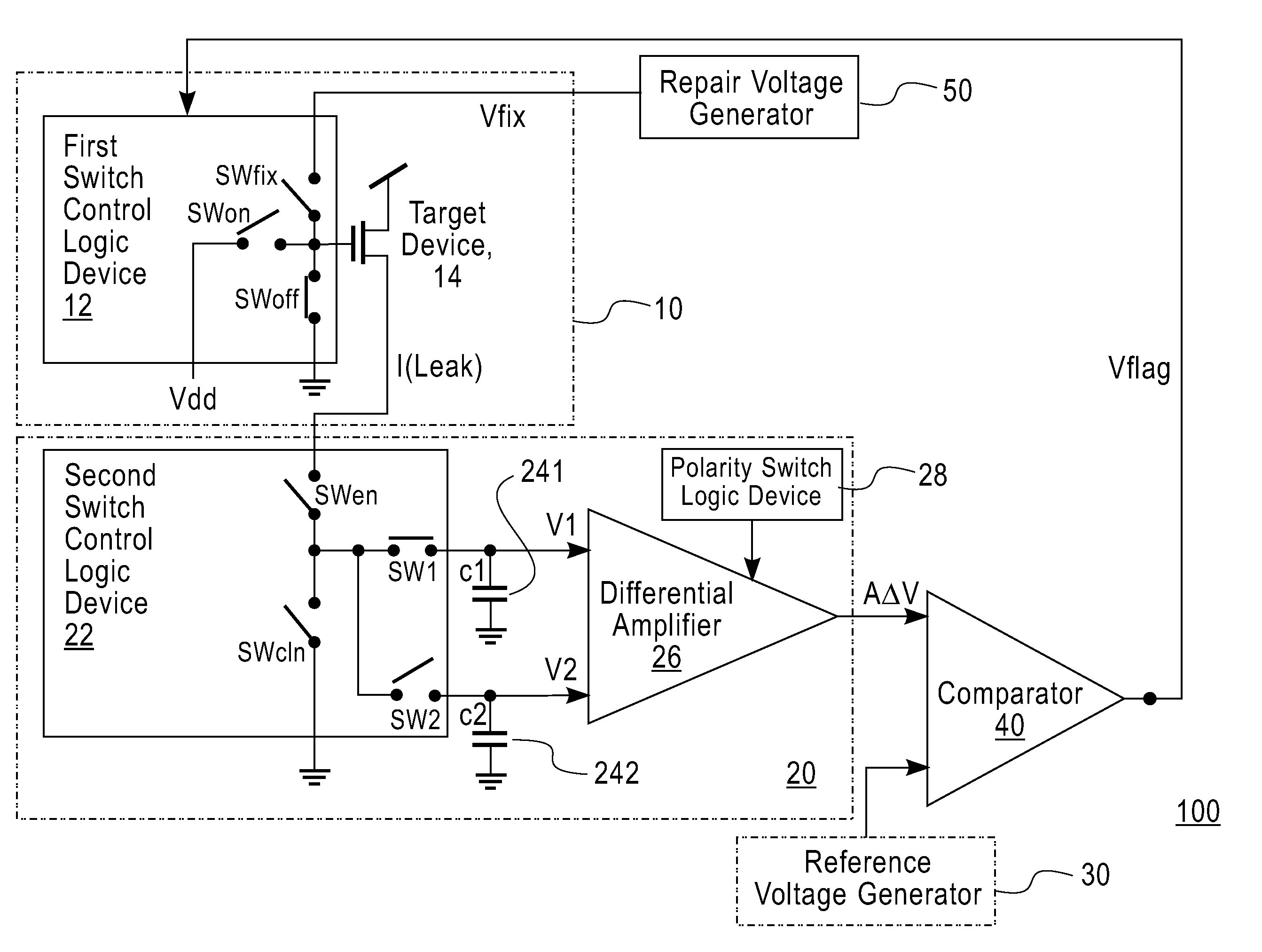
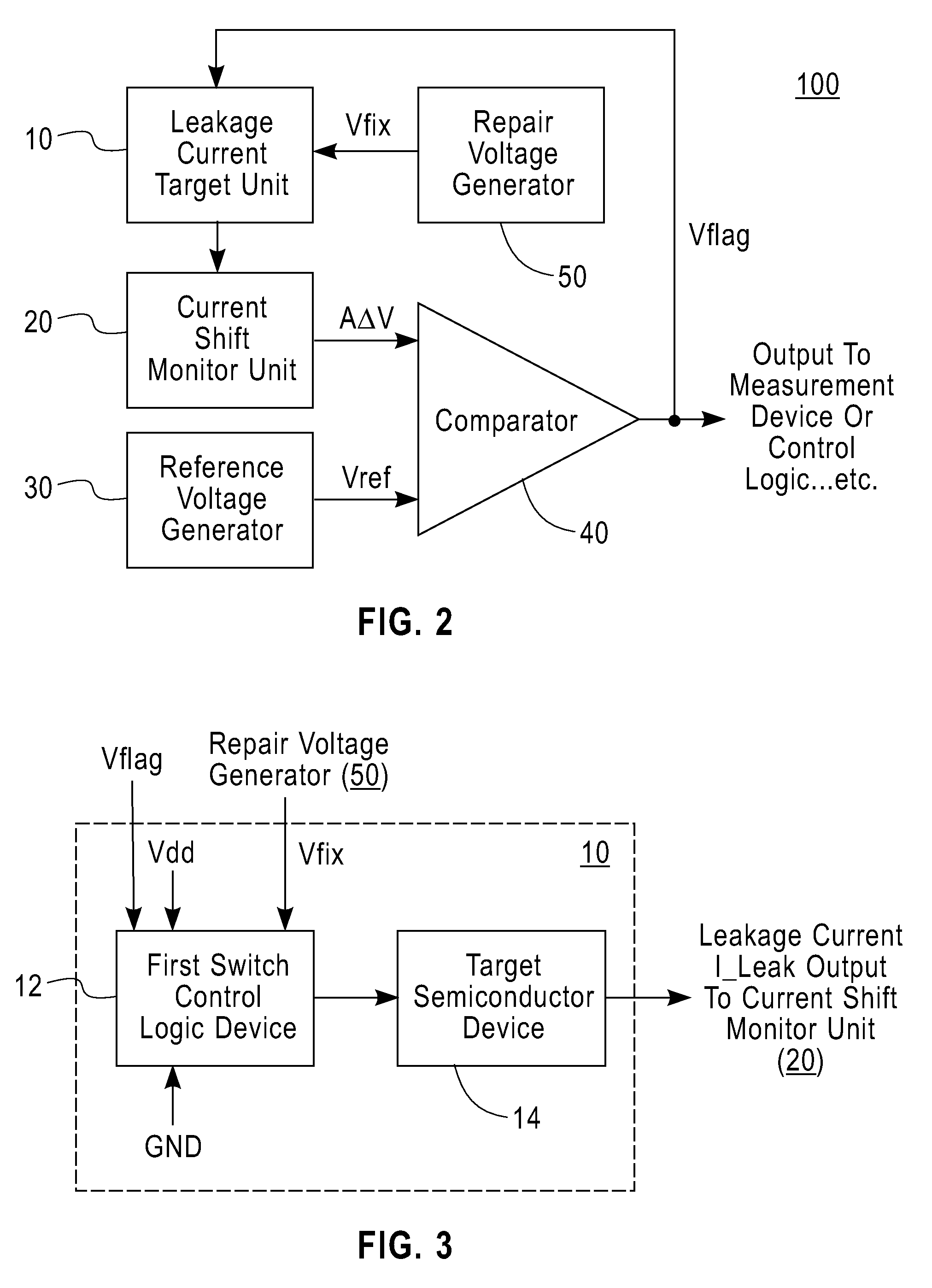
[0045]One or more embodiments of the invention provide a method and circuit for detecting and mitigating leakage current shift in a semiconductor device, particularly in a MOSFET device, before catastrophic leakage current runaway occurs.

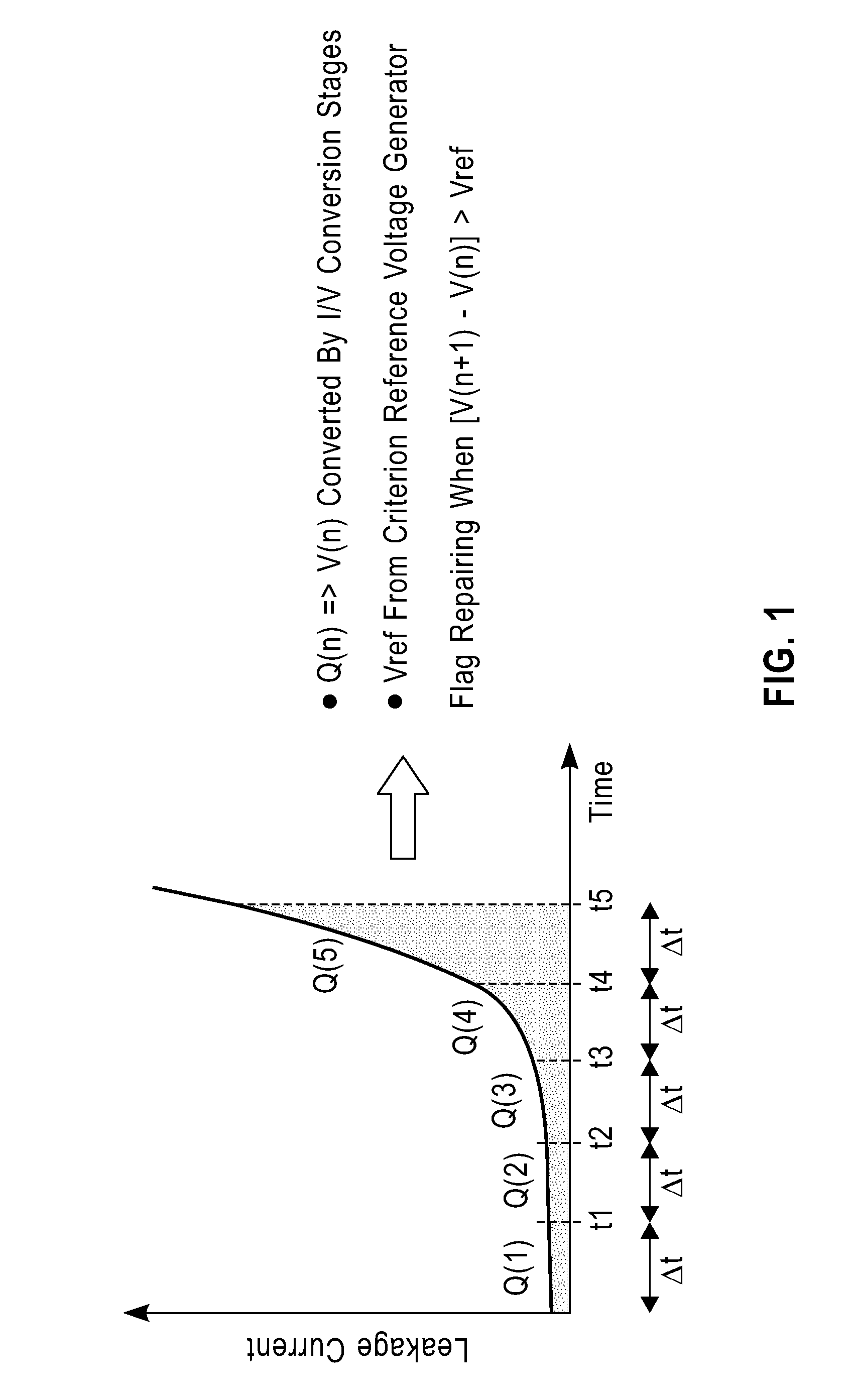
[0046]As shown in FIG. 1, a charge (Q) due to leakage current in a target semiconductor device in a leakage current target is collected for a plurality of discrete temporal periods (Δt). According to a sample embodiment, the semiconductor device is a MOSFET device in dormant mode. During a first temporal period t1, a second temporal periods t2, and a third temporal period t3, the charge due to leakage for each temporal period is not significantly different from one temporal period to the next (i.e., less than about 25% change) so there is no significant leakage current shift. During a fourth temporal period t4, however, the charge Q due to leakage current is significantly larger than during the previous temporal period t3 (i.e., greater than 200% ch...


PUM


Abstract

A dormant mode target semiconductor device within a leakage current target unit is identified for mitigating leakage current to prevent it from reaching catastrophic runaway. A leakage current shift monitor unit is electrically connected to the output node of the leakage current target unit and collects leakage current from the selected target semiconductor device for two consecutive predefined temporal periods and measures the difference between the collected leakage currents. A comparator receives and compares the outputs of the current shift monitor unit and a reference voltage generator. The comparator propagates an alert signal to the leakage current target unit when the leakage voltage output from the leakage current shift monitor unit exceeds the reference voltage, a condition that indicates that the leakage current is about to approach catastrophic runaway levels. This alert signal switches the target semiconductor device to an active mode for leakage mitigation, which includes a repair voltage from a repair voltage generator applied to the gate of the target semiconductor device.

Description

FIELD OF THE INVENTION[0001]The present invention relates to the field of semiconductors and more particularly to an apparatus and method for mitigating leakage current in a semiconductor device before catastrophic leakage current runaway occurs. It should be understood that while the apparatus and method of the invention described herein relate to semiconductor devices generally, specific emphasis is placed on the present invention's application to metal oxide semiconductor field effect transistor (MOSFET) devices.BACKGROUND OF THE INVENTION[0002]Leakage current runaway is a catastrophic phenomenon that occurs in MOSFET devices during dormant mode when a MOSFET device is biased with full operating voltage (Vdd) across source and drain nodes while gate voltage is switched off. Normally, the leakage current in a dormant MOSFET device does not change with time. However, if the device channel length is sufficiently short, the leakage current, especially the drain induced barrier lower ...

Claims


Application Information

Patent Timeline
Patent Type & Authority Patents(United States)
IPC IPC(8): G05F1/10G01R31/26
CPCH03K17/0822
Inventor GUO, JONG-RUHSU, LOUIS LU-CHENJOSHI, RAJIV VASANTWANG, PING-CHUANYANG, ZHIJIAN
Owner GLOBALFOUNDRIES INC
Why Eureka
Try Eureka