Integrated circuit structure having bottle-shaped isolation

a technology of integrated circuits and isolation channels, which is applied in the direction of basic electric elements, electrical equipment, semiconductor devices, etc., can solve the problems of high cost or low throughput of most of these, and achieve the effect of reducing the problem of substrate leakag

Active Publication Date: 2011-04-26
PROMOS TECH INC
View PDF4 Cites 8 Cited by
  • Summary
  • Abstract
  • Description
  • Claims
  • Application Information

AI Technical Summary

Benefits of technology

[0009]One aspect of the present invention provides an integrated circuit structure having a bottle-shaped shallow trench isolation and method for preparing the same, which can reduce the substrate leakage problem in the conventional planar transistor and prevent the floating body effect occurring in the conventional silicon-on-insulator substrate.
[0013]The conventional integrated circuit structure still suffers from various types of current leakage through the wide portion of the semiconductor substrate directly below the gate and the source / drain regions of the planar transistor. In contrast, according to the integrated circuit structure of the present invention, the portion of the semiconductor substrate directly below the device region with the transistor therein is much narrower, which can effectively solve the current leakage problem of the conventional integrated circuit structure.
[0014]The silicon-on-insulator (SOI) structure is widely used to solve the current leakage problem of the conventional planar transistor; however, there is a major disadvantage of the SOI structure known as the “floating body effect” originating from the accumulation of charges and lack of thermal conductivity, which needs to be resolved by designing an extra current path. In contrast, the integrated circuit structure of the present invention inherently possesses a current path, which can effectively solve the floating body effect of the conventional SOI structure, without designing an extra current path.

Problems solved by technology

The conventional methods of preparing the SOI structure include SIMOX, SIMNI, SmartCut™ and Nanocleave™; most of these are expensive or low in throughput.
In addition, there is a major disadvantage to the SOI structure known as the “floating body effect” originating from the accumulation of electric charge and lack of thermal conductivity, which needs to be resolved by designing an extra current path.

Method used


Image

  • Integrated circuit structure having bottle-shaped isolation
  • Integrated circuit structure having bottle-shaped isolation
  • Integrated circuit structure having bottle-shaped isolation

Examples


Embodiment Construction

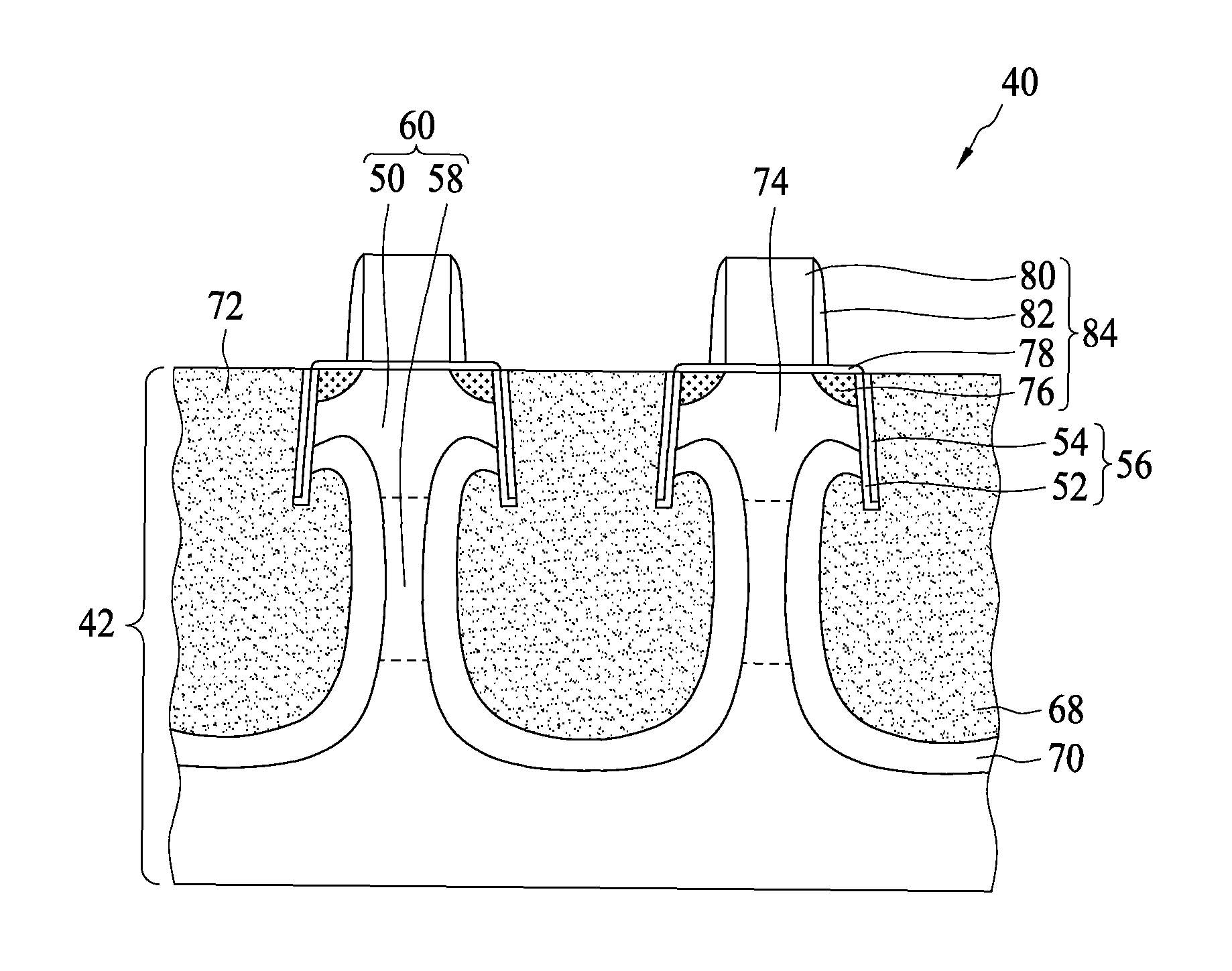
[0020]FIG. 5 to FIG. 12 illustrate a method for preparing an integrated circuit structure 40 according to one embodiment of the present invention. First, a plurality of top masks 48 are formed on a semiconductor substrate 42 such as the silicon substrate by the deposition process followed by the lithographic process and the etching process, and a dry etching process is then performed to remove a portion of the semiconductor substrate 42 not covered by the top masks 48 to form a plurality of protrusions 50. Each of the top masks 48 includes an oxide layer 44 and a nitride layer 46.

[0021]Referring to FIG. 6, a thermal treating process is performed to form a wall oxide layer (dielectric layer) 52 covering the sidewalls of the protrusions 50 and the surface of the semiconductor substrate 42, and a deposition process is then performed to form a liner nitride layer (dielectric layer) 54 on the wall oxide layer 52. Subsequently, an etching process such as an etching back process is perform...


PUM


Abstract

An integrated circuit structure comprises a semiconductor substrate, a device region positioned in the semiconductor substrate, an insulating region adjacent to the device region, an isolation structure positioned in the insulating region and including a bottle portion and a neck portion filled with a dielectric material, and a dielectric layer sandwiched between the device region and the insulation region.

Description

BACKGROUND OF THE INVENTION[0001](A) Field of the Invention[0002]The present invention relates to an integrated circuit structure and method for preparing the same, and more particularly, to an integrated circuit structure having a bottle-shaped shallow trench isolation and method for preparing the same.[0003](B) Description of the Related Art[0004]Conventional integrated circuit fabrication processes use a local oxidation of silicon (LOCOS) technique or shallow trench isolation (STI) technique to electrically isolate wafer-mounted electronic devices from each other, so as to avoid short circuits and cross interference. Due to the LOCOS technique's forming a field oxide layer covering a larger wafer area and also because it forms a “bird's beak” pattern, advanced integrated circuit fabrication generally selects the STI technique to electrically isolate electronic devices.[0005]FIG. 1 to FIG. 4 illustrate a method for preparing an integrated circuit structure 10 having a planar metal...

Claims


Application Information

Patent Timeline
Patent Type & Authority Patents(United States)
IPC IPC(8): H01L21/70
CPCH01L21/76232H01L21/7624H01L21/76264H01L2924/0002H01L2924/00
Inventor WU, HSIAO CHETSAI, WEN LI
Owner PROMOS TECH INC
Why Eureka
Try Eureka