High throughput measurement system

a measurement system and high throughput technology, applied in the field of metalrology, can solve the problems of inability to meet the requirements of the substrate layer post-polishing thickness, and inability to meet the requirements of the substrate layer after polishing

Inactive Publication Date: 2011-05-31
APPLIED MATERIALS INC
View PDF73 Cites 12 Cited by
  • Summary
  • Abstract
  • Description
  • Claims
  • Application Information

AI Technical Summary

Benefits of technology

[0016]Possible advantages of implementations of the invention can include one or more of the following. A library of spectra can be assembled, and the spectra can be associated with physical properties of the substrate. Spectra-based endpoint determination can be made in-situ with greater speed and accuracy, and variations in the post-polishing thickness of the substrate layer can be reduced. Spectra-based measurements of substrate characteristics can be made by in-line monitoring systems with great speed.

Problems solved by technology

However, this metrology process can be time-consuming, and the metrology equipment can be costly.
One problem in CMP is determining whether the polishing process is complete (i.e., whether a substrate layer has been planarized to a desired flatness or thickness).
Therefore, for some applications, determining the polishing endpoint merely as a function of polishing time can lead to unacceptable variations in the post-polishing thickness of the substrate layer.
However, removal of the substrate from the polishing apparatus for transportation to an in-line or stand-alone metrology station can lead to an unacceptable reduction in throughput.
However, measurements using such an in-situ system usually cannot be precisely positioned at a desired measurement location due to the motion of the substrate relative to the sensor, and the measurements can be less accurate due to noise generated by the polishing environment (e.g., absorption of light by slurry), the limited time available for measurements, and the need for real-time processing of the sensor data.

Method used


Image

  • High throughput measurement system
  • High throughput measurement system
  • High throughput measurement system

Examples


Embodiment Construction

8]FIG. 11 shows a method for using spectrum based endpoint determination to determine an endpoint of a polishing step.

[0029]FIG. 12 is a top view of an exemplary substrate processing system having an in-line spectrographic monitoring system.

[0030]FIG. 13 is a perspective view of an interior of an exemplary factory interface module.

[0031]FIG. 14 is a side view of an exemplary factory interface module having an in-line spectrographic monitoring system.

[0032]FIG. 15 illustrates an exemplary path of an optical probe of the in-line spectrographic monitoring system across a reference substrate during spectrographic measurements for library generation.

[0033]FIG. 16 illustrates an exemplary path of an optical probe of the in-line spectrographic monitoring system across a device substrate during spectrographic measurements for data collection for processing control.

[0034]Like reference symbols in the various drawings indicate like elements.

DETAILED DESCRIPTION

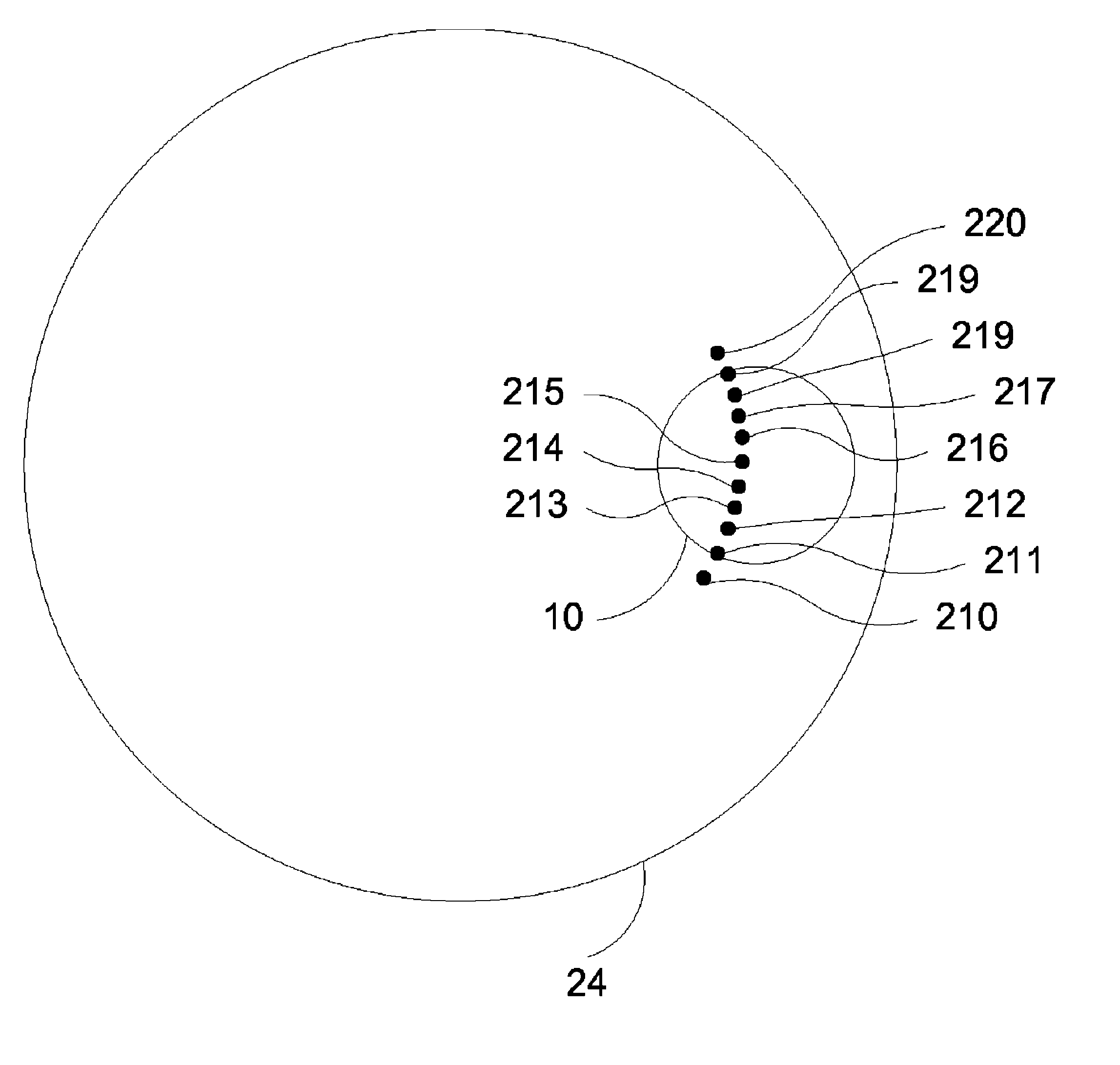
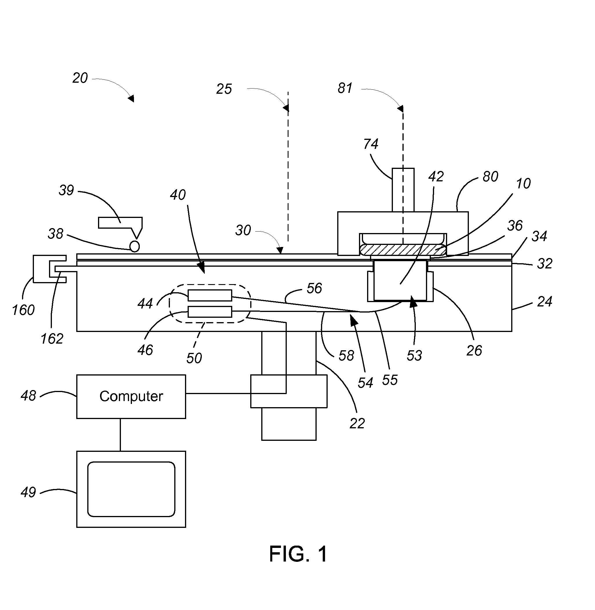
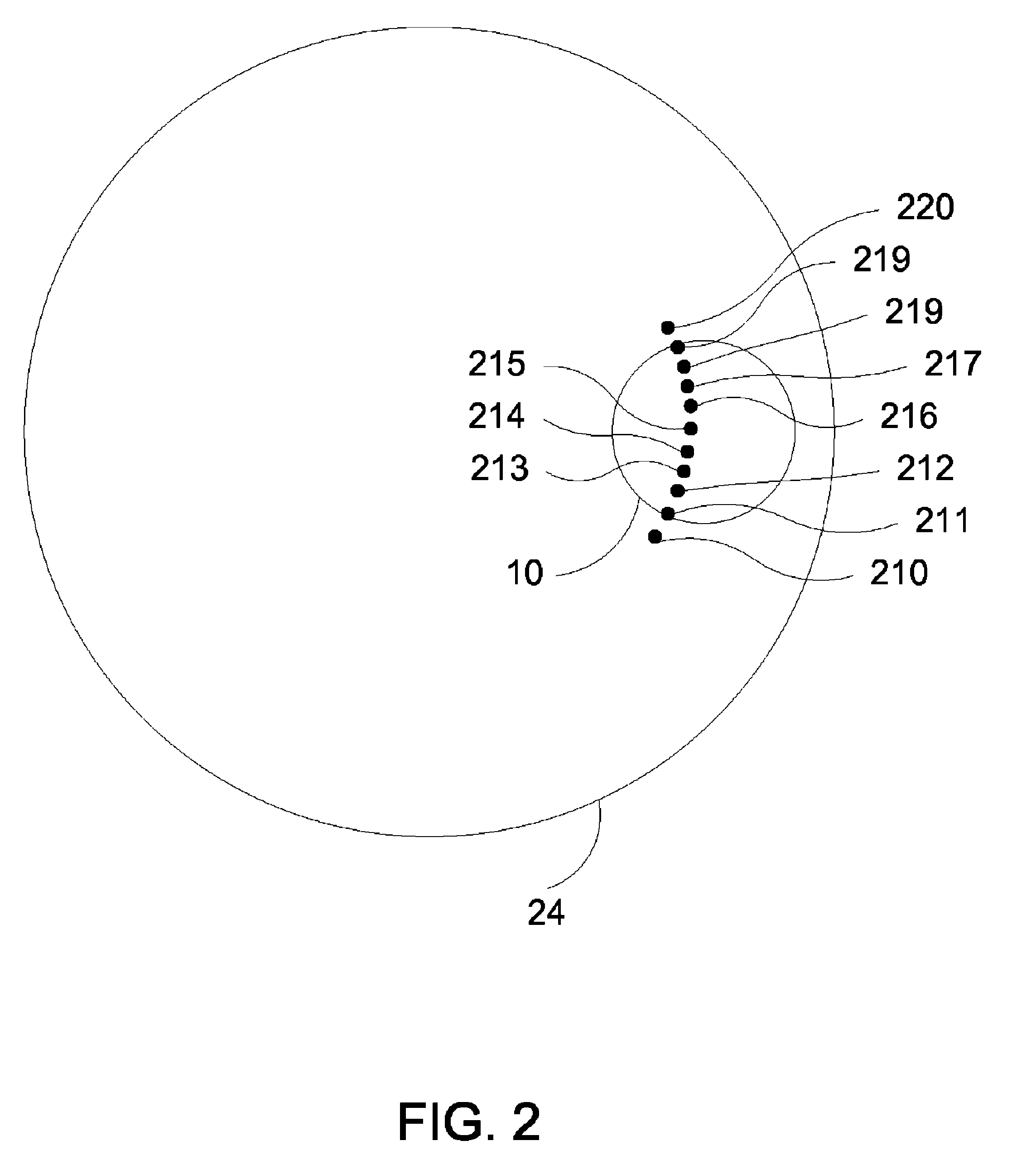
[0035]Referring to FIG. 1, one o...


PUM


Abstract

A substrate processing system includes a processing module to process a substrate, a factory interface module configured to accommodate at least one cassette for holding the substrate, a spectrographic monitoring system positioned in or adjoining the factory interface module, and a substrate handler to transfer the substrate between the at least one cassette, the spectrographic monitoring system and the processing module.

Description

CROSS-REFERENCE TO RELATED APPLICATIONS[0001]Under 35 U.S.C. §119(e)(1), this application claims the benefit of prior U.S. Provisional Application 60 / 949,498, filed Jul. 12, 2007, and U.S. Provisional Application 60 / 909,639, filed Apr. 2, 2007.TECHNICAL FIELD[0002]This invention relates to metrology, and in one aspect to optical monitoring of substrates during a chemical mechanical polishing process.BACKGROUND[0003]An integrated circuit is typically formed on a substrate by the sequential deposition of conductive, semiconductive, or insulative layers on a silicon wafer. One fabrication step involves depositing a filler layer over a non-planar surface and planarizing the filler layer. For certain applications, the filler layer is planarized until the top surface of a patterned layer is exposed. A conductive filler layer, for example, can be deposited on a patterned insulative layer to fill the trenches or holes in the insulative layer. After planarization, the portions of the conduct...

Claims


Application Information

Patent Timeline
Patent Type & Authority Patents(United States)
IPC IPC(8): G01J3/40
CPCG01N21/253G01N21/31H01L21/67766H01L21/67207H01L21/67253H01L21/67161H01L21/00H01L21/304H01L22/00
Inventor RAVID, ABRAHAMSWEDEK, BOGUSLAW A.BENVEGNU, DOMINIC J.DAVID, JEFFREY DRUEQIAN, JUNHUEY, SIDNEY P.CARLSSON, INGEMARKARUPPIAH, LAKSHMANANLEE, HARRY Q.
Owner APPLIED MATERIALS INC
Why Eureka
Try Eureka