

Nonvolatile semiconductor memory device which realizes “1” write operation by boosting channel potential
a semiconductor memory and channel potential technology, applied in static storage, digital storage, instruments, etc., can solve the problems of erroneous write operation and erroneous write operation with respect to the cell connected to the word line wlb>0/b>, and achieve the effect of preventing the occurrence of an erroneous write operation
- Summary
- Abstract
- Description
- Claims
- Application Information
AI Technical Summary
Benefits of technology
Problems solved by technology
Method used
Image

Examples
first embodiment
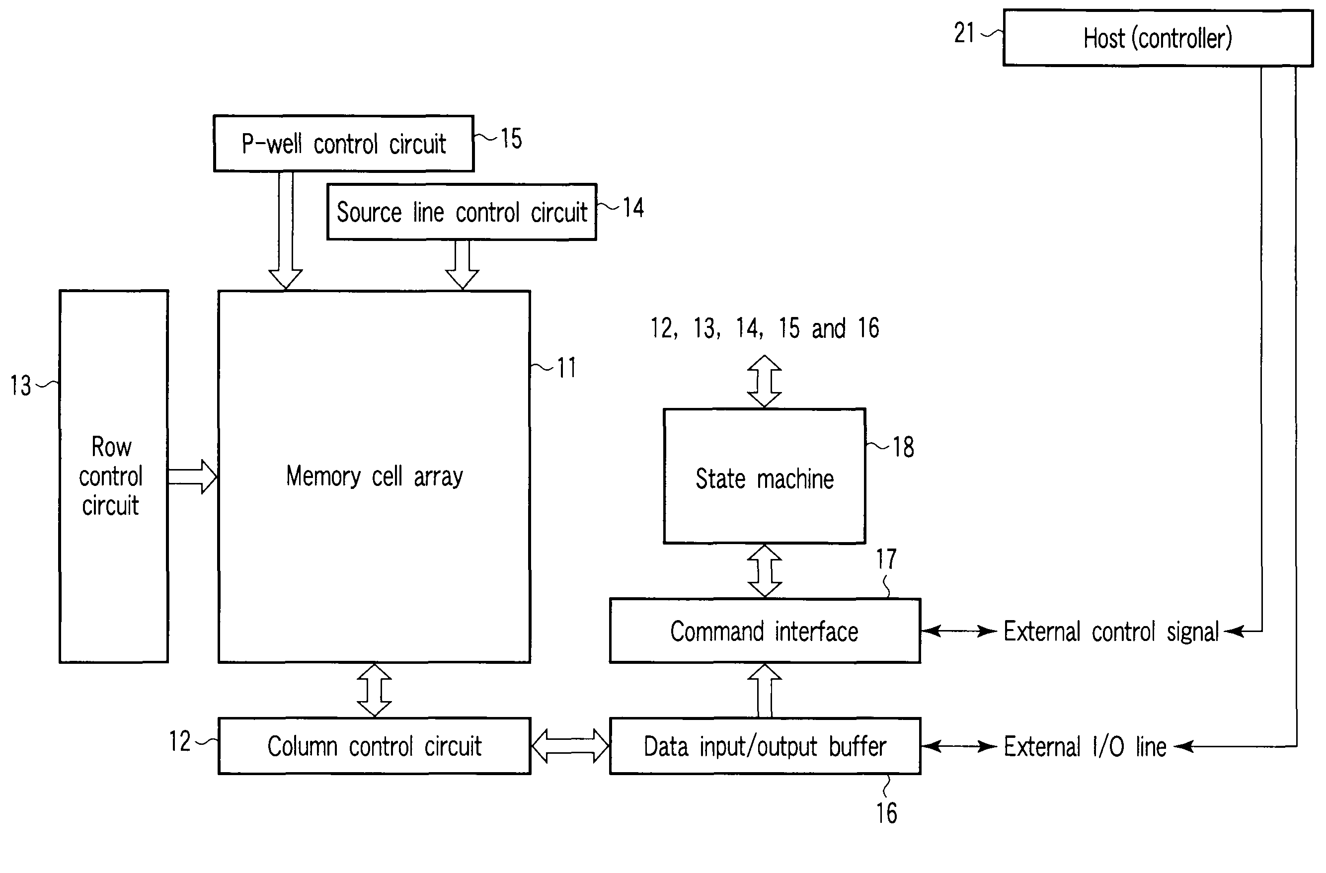
[0023]FIG. 1 shows an example of the configuration of a nonvolatile semiconductor memory device according to a first embodiment of this invention. In the present embodiment, a NAND flash memory is taken as an example and explained as the nonvolatile semiconductor memory device.
[0024]In FIG. 1, a memory cell array 11 is configured to have a plurality of flash memory cells arranged in a matrix form. A column control circuit 12 and row control circuit 13 are provided near the memory cell array 11. The column control circuit 12 controls bit lines to erase data held in the memory cell, write data into the memory cell or reads out data from the memory cell. The row control circuit 13 selectively applies potentials required for erasing, writing and readout to word lines and select gate transistors.
[0025]Further, a source line control circuit 14 which controls the potential of the source line and a P-well control circuit 15 which controls the potential of a p-type well in which the memory c...
second embodiment
[0058]FIG. 10 illustrates a “1” write operation performed in a nonvolatile semiconductor memory device according to a second embodiment of this invention. In the present embodiment, a case wherein a “1” write operation is performed with respect to a memory cell MC0 in a NAND flash memory is explained. In this example, a case wherein a source-side select gate transistor SGS-Tr is controlled to discharge channel precharge potential is explained.
[0059]When a word line WL0 is selected, first, a drain-side select gate transistor SGD-Tr is turned on by potential Vsg from a row control circuit 13 to precharge the channel. After this, the source-side select gate transistor SGS-Tr is turned on by potential Vsgs_vth from the row control circuit 13. As a result, the potential precharged on the channel is freely discharged.
[0060]Thus, by controlling the boost voltage, an exact “1” write operation for memory cell MC0 is performed while occurrence of an erroneous write operation is suppressed. Th...
third embodiment
[0064]FIG. 11 illustrates a “1” write operation in a nonvolatile semiconductor memory device according to a third embodiment of this invention. In the present embodiment, a case wherein a “1” write operation is performed with respect to a memory cell MC0 in a NAND flash memory is explained. In this example, a case wherein a drain-side select gate transistor SGD-Tr is controlled to control boost voltage (initial charging voltage of the channel) is explained.
[0065]When a word line WL0 is selected, first, the drain-side select gate transistor SGD-Tr is turned on to precharge the channel. At this time, the channel precharge potential can be controlled by changing the gate voltage of the drain-side select gate transistor SGD-Tr.
[0066]For example, when potential is transferred from a bit line BL to the channel, potential Vsgd_vth is supplied from a row control circuit 13 as the gate voltage of the drain-side select gate transistor SGD-Tr. Thus, the channel can be precharged to “potential ...
PUM
 Abstract
Description
Claims
Application Information