MEMS switch and manufacturing method thereof

a mechanical system and switch technology, applied in the direction of adjustable resistors, semiconductor devices, relays, etc., can solve the problems of deteriorating the accuracy of the voltage value that can be obtained, increasing the resistance value of the resistance, and increasing the temperature difference between the resistances used in the voltage-dividing circuit. achieve the effect of small chip area, high accuracy of operation, and temperature differences

Inactive Publication Date: 2011-06-07
SEIKO EPSON CORP
View PDF19 Cites 14 Cited by
  • Summary
  • Abstract
  • Description
  • Claims
  • Application Information

AI Technical Summary

Benefits of technology

[0010]Some embodiments provide a MEMS switch with which a highly accurate operation is possible by making an increase of the area where a chip occupies and the temperature differences in the chip as small as possible, with which an application to a high-frequency band is possible by making the increase of the chip area small and with which the operation in the high-frequency band is stabilized.

Problems solved by technology

Consequently, temperature differences among resistances used in the voltage-dividing circuit become larger and differences in the resistance values of the resistances increase due to the temperature coefficient of each resistance.
This deteriorates the accuracy of the voltage value that can be obtained from the voltage-dividing circuit.
An operational frequency therefore decreases since it is proportional to the inverse of the wavelength, and this limits the operational bandwidth in a high-frequency band.
The amount of reflection from the short-stub or the open-stub will become large when the Q value is high, making the operation in the high-frequency band unstable.

Method used


Image

  • MEMS switch and manufacturing method thereof
  • MEMS switch and manufacturing method thereof
  • MEMS switch and manufacturing method thereof

Examples


first embodiment

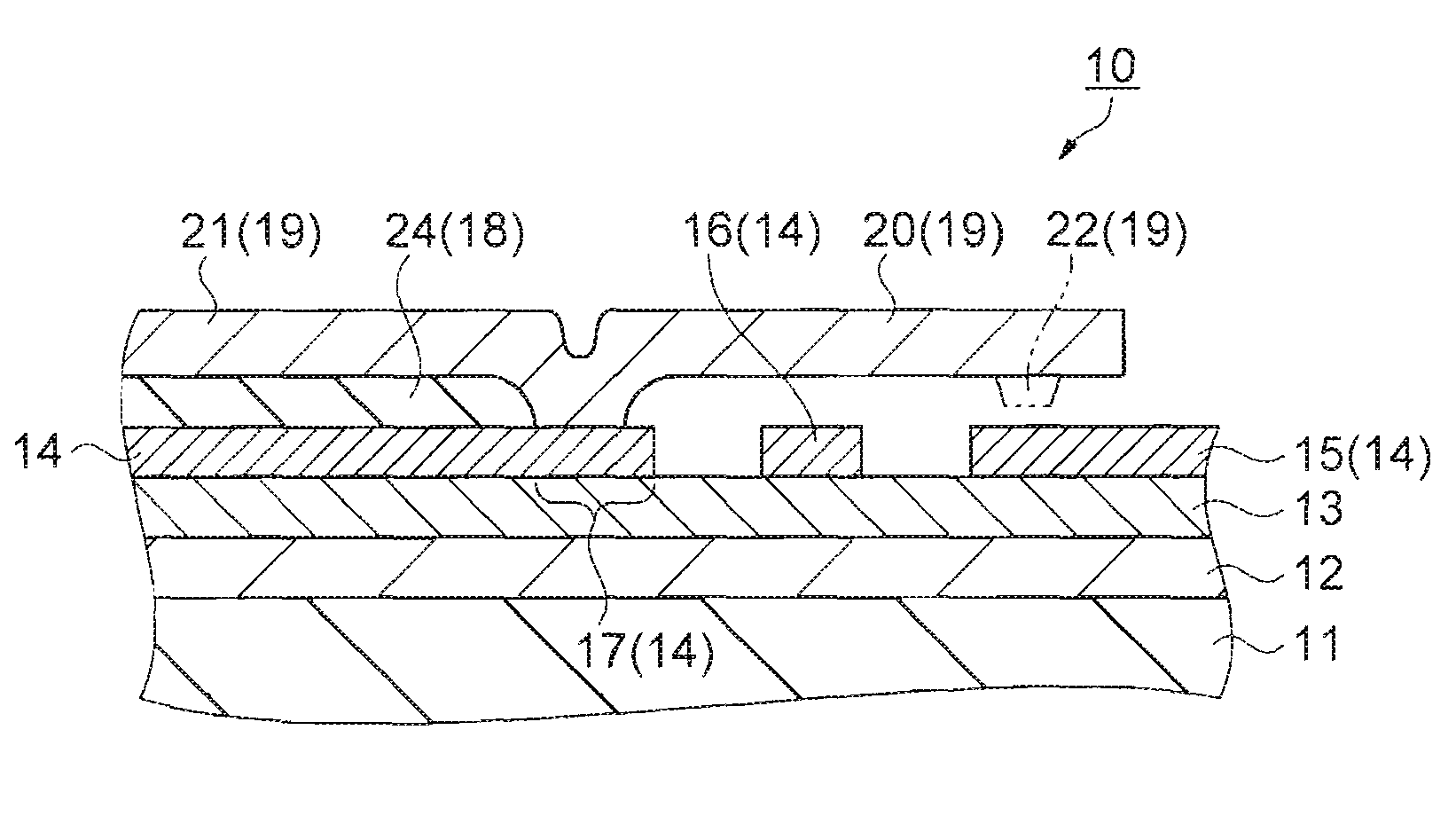
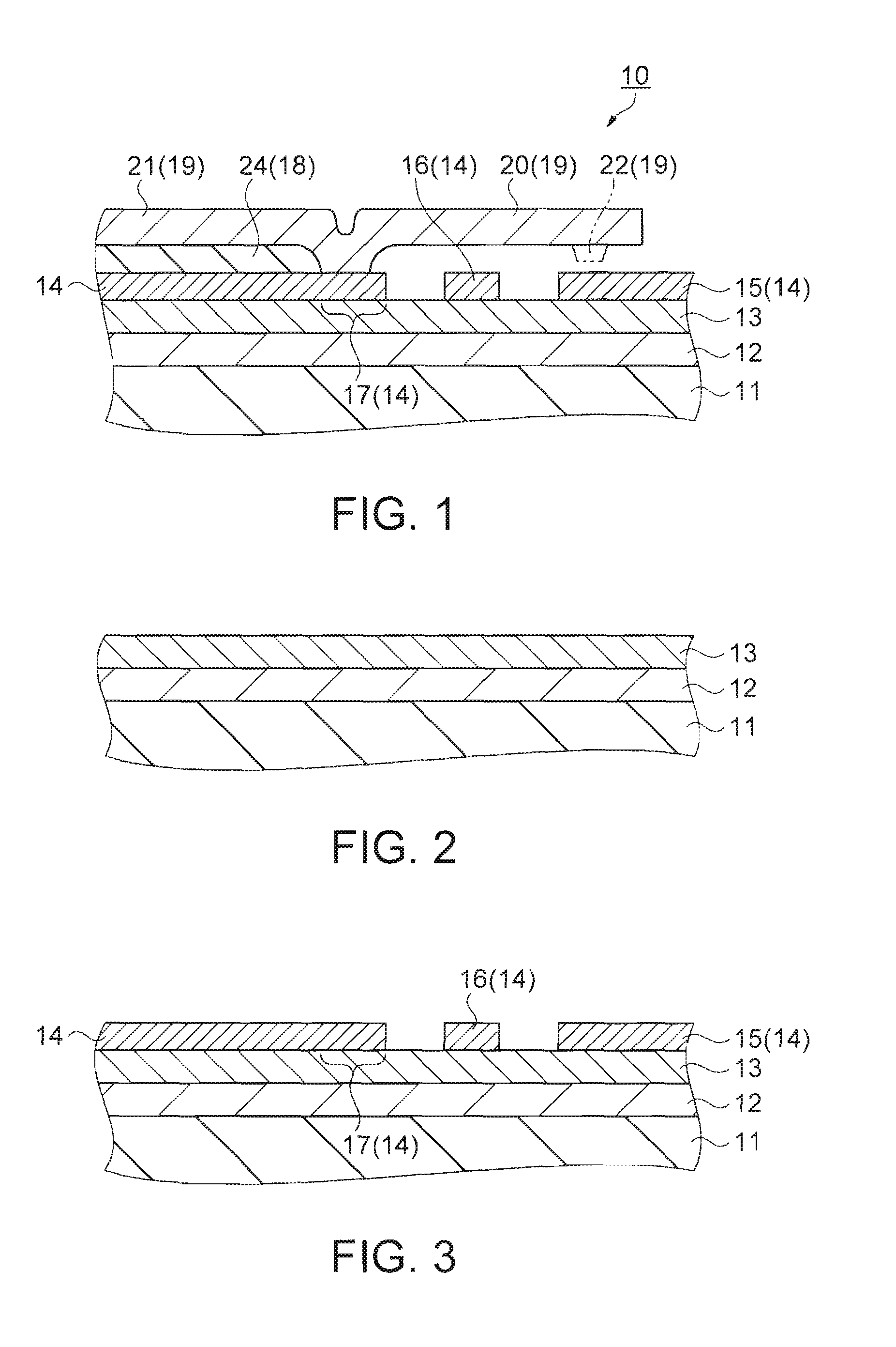
[0054]FIG. 1 is a schematic sectional view of a micro-electro mechanical system (MEMS) switch.

[0055]A MEMS switch 10 includes an oxide silicon layer 12 formed on a silicon substrate 11 and a silicon nitride layer 13 formed on the oxide silicon layer 12.

[0056]The MEMS switch 10 further includes a fixed electrode 15 provided on the silicon nitride layer 13, a driving electrode 16 which controls connection / disconnection of the MEMS switch 10, and a supporting member 17 that supports a movable electric resistor 20. The fixed electrode 15 is formed by etching a first polysilicon layer 14.

[0057]The movable electric resistor 20 supported by the supporting member 17 is situated between the fixed electrode 15 and the driving electrode 16 which controls the connection / disconnection of the MEMS switch 10 with certain gaps therebetween.

[0058]Here, a strip-shaped protrusion 22 can be further provided around an open end of the movable electric resistor 20. The strip-shaped protrusion 22 contacts ...

second embodiment

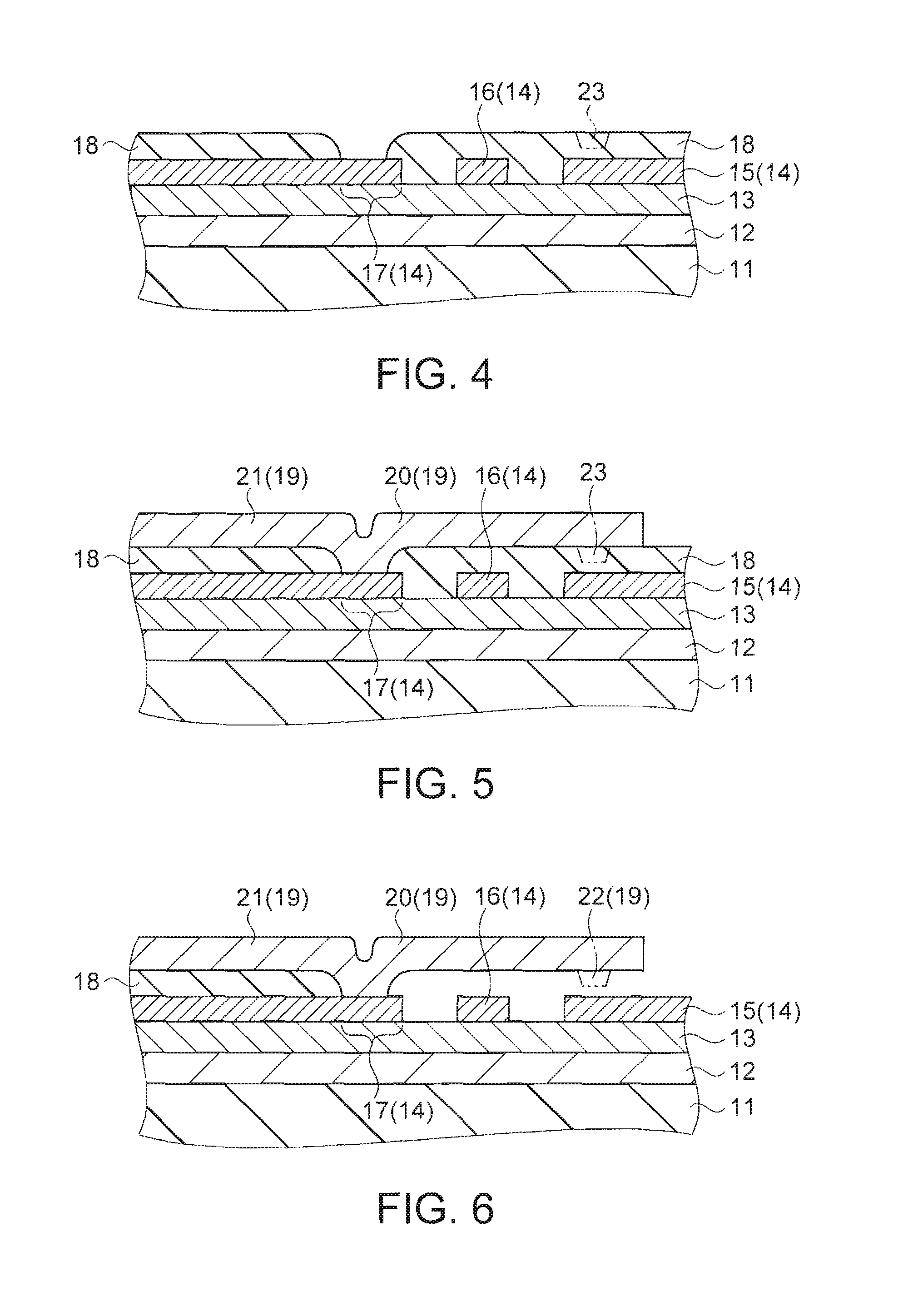
[0069]A manufacturing process of the MEMS switch 10 shown in FIG. 1 will now be described as a second embodiment. FIGS. 2 through 6 are sectional views schematically showing the manufacturing process of the MEMS switch according to the second embodiment.

[0070]Referring to FIG. 2, the oxide silicon layer 12 which relives the stress is firstly formed on the silicon substrate 11 in Step 1 of the manufacturing process of the MEMS. Thermal oxidation, chemical deposition or the like can be used to form the oxide silicon layer. The silicon nitride layer 13 which is an insulating layer protecting the oxide silicon layer 12 from an etching solution is subsequently formed. The silicon nitride layer can be formed by for example a chemical vapor deposition (CVD) method. A glass substrate, a quartz substrate, a silicon-on-insulator (SOI) substrate and compound semiconductor substrates may be used instead of the silicon substrate 11.

[0071]Referring to FIG. 3, the first polysilicon layer 14 which ...

third embodiment

[0078]A voltage-dividing circuit using the MEMS switch will be now described as a third exemplary embodiment. FIG. 7A is schematic plan view of a voltage-dividing circuit 30 which is formed by using the MEMS switch 10. FIG. 7B is equivalent circuit schematic diagram of the voltage-dividing circuit 30. The reference numeral “10A” in FIG. 7B denotes an equivalent circuit of the MEMS switch 10.

[0079]The voltage-dividing circuit 30 has a resolution of 8-bit and an output voltage is represented by the following formula:

Vo=Vref×(⅓)×(B1 / 20+B2 / 21 . . . +B8 / 2(8−1))

Wherein Vref is an applied voltage, a most significant bit (MSB) is B1 and a least significant bit (LSB) is B8. It supposes that B1−B8 is “1” when they are coupled in the Vref side and B1−B8 is “0” when they are coupled in the ground side.

[0080]The accuracy of the voltage division by the voltage-dividing circuit 30 is dependent on the fluctuation of the resistance ratio. However, the accuracy will be not affected when each resistan...


PUM

PropertyMeasurementUnit
electric resistanceaaaaaaaaaa
electric currentaaaaaaaaaa
impedanceaaaaaaaaaa

Abstract

A micro-electro mechanical system (MEMS) switch includes a fixed electrode formed on a substrate, and a movable electric resistor formed on the substrate, the movable electric resistor serving as an electric resistor that divides an electric potential where the MEMS switch is set to a conduction state.

Description

CROSS-REFERENCE TO RELATED APPLICATION[0001]This application claims priority from Japanese Patent Application Serial No. 2006-212915, filed in the Japanese Patent Office on Aug. 4, 2006, the entire disclosure of which is hereby incorporated by reference in its entirety.BACKGROUND[0002]1. Technical Field[0003]Some embodiments of the present invention relates to a micro-electro mechanical system (MEMS) switch and a manufacturing method thereof.[0004]2. Related Art[0005]A MEMS switch is a switch having a minute structure formed on a substrate made of semiconductor or the like by using semiconductor manufacturing technologies. The MEMS switch has a fixed electrode fixed on the substrate and a movable electrode having a structure such as a cantilever beam, a doubly-supported beam, a diaphragm and the like. An on / off action of the MEMS switch is performed by utilizing an electrostatic force or the like.[0006]JP-T-2005-512830 is a first example of related art and JP-A-2005-124126 is a seco...

Claims


Application Information

Patent Timeline
Patent Type & Authority Patents(United States)
IPC IPC(8): H01H51/22
CPCH01C10/50H01H59/0009Y10T29/49105H01H59/00H01L29/00
Inventor WATANABE, TORUSATO, AKIRAINABA, SHOGOMORI, TAKESHI
Owner SEIKO EPSON CORP
Why Eureka
Try Eureka