Method for multi-cycle path and false path clock gating

a multi-cycle path and false path technology, applied in the field of chip design, can solve the problems of large amount of standby or static current, limit power consumption, and increase static power consumption with each new technology, and achieve the effect of reducing switching power consumption and consuming less power

Active Publication Date: 2011-06-07
SYNOPSYS INC
View PDF14 Cites 9 Cited by
  • Summary
  • Abstract
  • Description
  • Claims
  • Application Information

AI Technical Summary

Benefits of technology

Techniques for a method for automatic clock gating of multi-cycle path and false paths are described herein. Embodiments of the present invention are able to reduce the switching power consumed on electronic circuits having one or more functional blocks. In one embodiment of the present invention, logic circuit blocks that can be clock-gated are identified using a design automation tool. Clock gating logic is inserted automatically thus producing a circuit which consumes less power. The techniques described herein may be extended for automatic insertion of power gating logic.

Problems solved by technology

Accordingly, one concern to chip designers is the limitation of power consumption.
Static power consumption has increased with each new technology due to higher leakage currents.
These leakage currents lead to a large amount of standby or static current, even though no switching is taking place.
Operating a chip at a slower speed, however, leads to a corresponding lower performance.
Lower performance is not a viable option given the insatiable customer demand for higher performance, and thus greater processing power.
However, as the supply voltage is reduced the performance also reduces, creating a dilemma for the chip designer.
The decision to perform clock gating and what logic circuits to gate has typically been a laborious, designer intensive job.
Given this significant effort and the fact that the amount of on chip logic has grown radically, obtaining a truly optimal gating arrangement has become problematic.
It is highly unlikely for any designer to identify all of the circuit portions which can be clock gated to save power and to properly implement the clock gating.
Further, a clock gating circuit itself occupies chip area and consumes additional power.
Clock gating of certain types of circuitry is more difficult than others.
One problem is that multi-cycle paths and false paths can consume power uselessly because they can consume power without providing a function calculation.

Method used


Image

  • Method for multi-cycle path and false path clock gating
  • Method for multi-cycle path and false path clock gating
  • Method for multi-cycle path and false path clock gating

Examples


case 0

{switch (state){ state—00( );break;case 1: state—01( );break;case 2: state—02( );break;case 3: state—03( );break;case 4: state—04( );break;default: state_error( )break;}

{

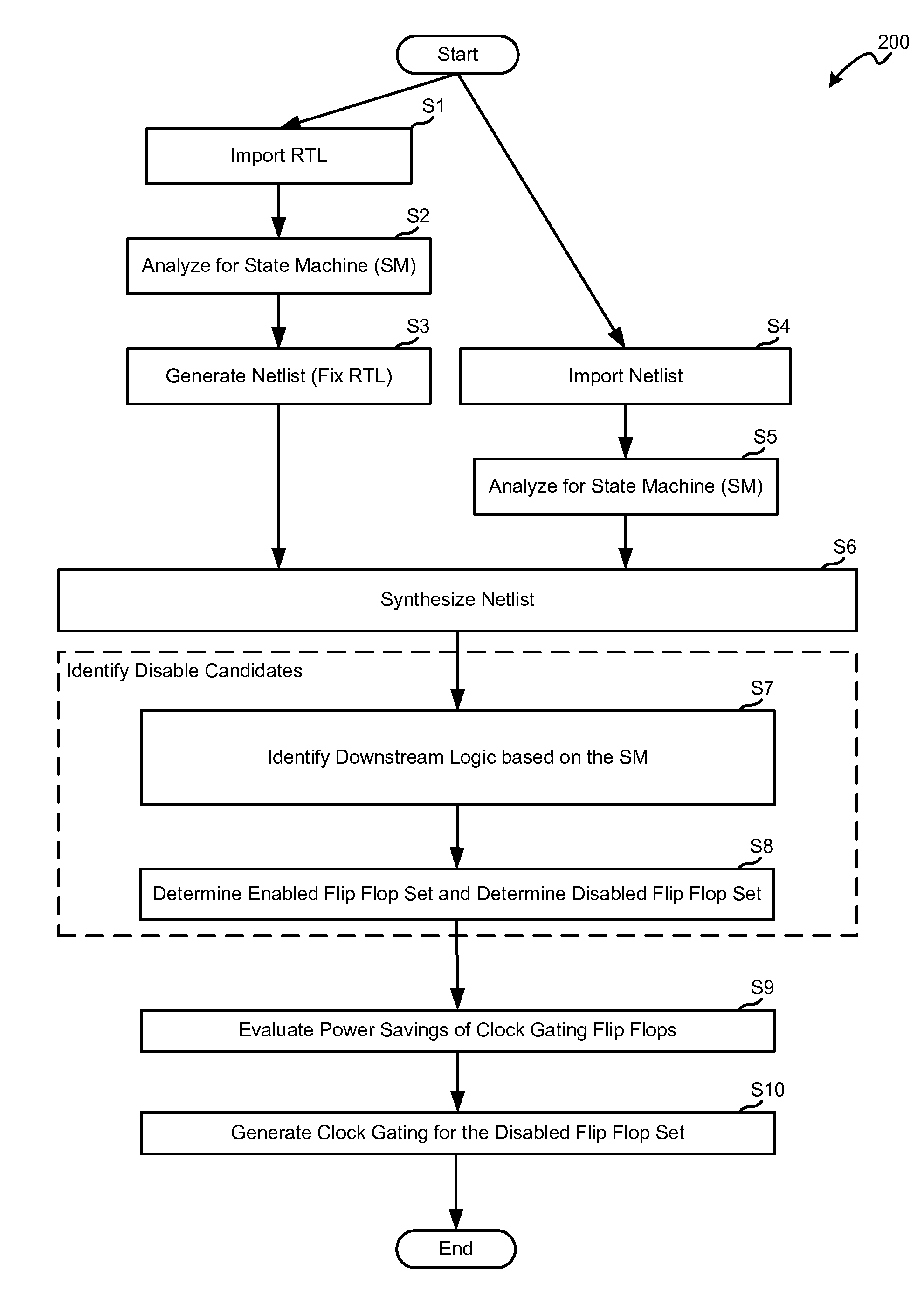
The imported RTL is examined for this and other RTL constructs, which are translated to the DFG, to determine state machines. More particularly, states comprising the state machine are identified by analyzing the DFG for statements which can be represented by a SM. For example, always and nested switch statements may be identified in the DFG. Other types of statements and structures which are known to be represented by state machines may also be identified. The states in the SM can be determined using the identified structure in the RTL. In the case of a always and nested switch structure, each case statement is identified as being a state in the SM and the registers that represent the case statement in the IC design are identified as state registers.

In addition to identifying the states, the state transitions may b...


PUM


Abstract

A power optimization method of deriving gated circuitry in an integrated circuit (IC) is provided. A design description of the IC is received and analyzed. A state machine is identified based on the analysis. One or more candidate blocks are determined to be capable of being disabled. At least one of the candidate blocks is selected based on one or more states of the state machine. A gating circuit is inserted for gating the selected candidate block(s). In another embodiment of power optimization, one or more state machines are identified and a synthesized netlist is generated. One or more candidate blocks in the synthesized netlist are determined to be capable of being disabled. At least one of the candidate blocks is selected based on one or more states in the state machine, and a gating circuit is inserted for gating the selected candidate block(s).

Description

BACKGROUND OF THE INVENTIONThis invention relates generally to the field of chip design and more particularly to a method for multi-cycle path and false path clock gating.Semiconductor chips are composed of complex electronic circuit arrangements. With each progressive generation of semiconductor technology the on-chip power utilized radically increases. Accordingly, one concern to chip designers is the limitation of power consumption. In order to reduce the chip power consumption, various circuit and architectural techniques have been employed. Both dynamic power and static power are of significant concern in today's technologies. Dynamic power is the power that is generated due to switching on the semiconductor chip. Static power consumption has increased with each new technology due to higher leakage currents. These leakage currents lead to a large amount of standby or static current, even though no switching is taking place.One method for reducing dynamic power has been the redu...

Claims


Application Information

Patent Timeline
Patent Type & Authority Patents(United States)
IPC IPC(8): G06F17/50
CPCG06F17/505G06F2217/78G06F30/327G06F2119/06
Inventor JIANG, YUNJIAN WILLIAMSRINIVASAN, ARVINDCHAUDHURI, SAMIT
Owner SYNOPSYS INC
Why Eureka
Try Eureka