

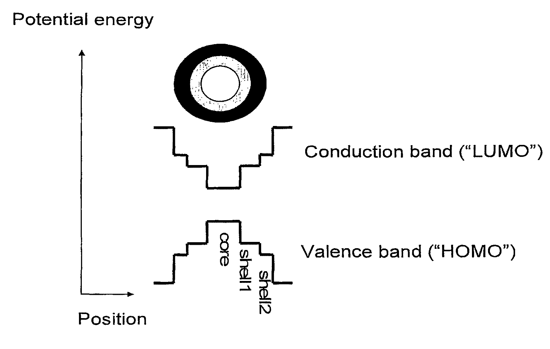
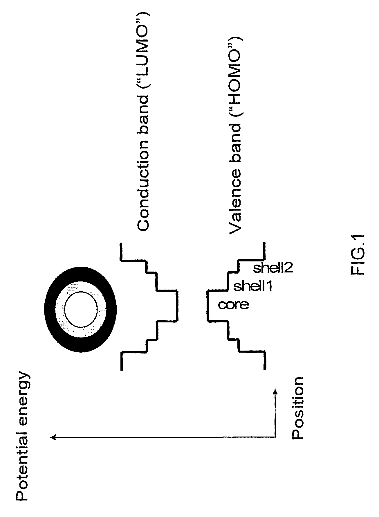
III-V semiconductor core-heteroshell nanocrystals
a technology of semiconductor cores and nanocrystals, which is applied in the field of manufacturing and using cores/multishell semiconductor nanocrystals, can solve problems such as the creation of defect sites, and achieve the effect of increasing their solubility
- Summary
- Abstract
- Description
- Claims
- Application Information
AI Technical Summary
Benefits of technology
Problems solved by technology
Method used
Image

Examples
Embodiment Construction
[0061]In a general procedure, the core / multishell structures of the invention are manufactured from quantum dots or III-V cores which are first dissolved in a non-coordinating solvent, such as 1-Hexadecene, Hexadecane, Heptadecane, 1-Octadecene, octadecane, Nonadecane, Eicosane, containing a long chained amine compound such as Decylamine, Dodecylamine, or Tributylamine, which serves as a capping ligand or with other ligands such as phosphines (for example trioctylphosphine, tributylphosphine, trioctylphosphine oxide and the like), or with thiols such as hexanethiol, benzenethiol, dodecanthiol and the like. The stock precursor solutions for the cations and anions of the shell materials are introduced into the hot reaction vessel in a sequential manner. As the reaction of one species is complete (half layer) the counter ion is inserted to complete the layer (full layer). This is followed by the growth of additional layers of the same shell, thus affording a shell of a required thickne...
PUM
| Property | Measurement | Unit |
|---|---|---|
| luminescence at a wavelength | aaaaa | aaaaa |
| wavelength | aaaaa | aaaaa |
| diameter | aaaaa | aaaaa |
Abstract
Description
Claims
Application Information