Method for manufacturing p type gallium nitride based device

a gallium nitride and gan technology, applied in the field of gan devices, can solve the problems of degrading the reliability of the device, and the method is limited in obtaining a sufficient characteristic of the ohmic contact, and achieve the effect of increasing the concentration of holes

Inactive Publication Date: 2011-06-21
THELEDS
View PDF5 Cites 5 Cited by
  • Summary
  • Abstract
  • Description
  • Claims
  • Application Information

AI Technical Summary

Benefits of technology

[0022]The method for manufacturing for the p-type gallium nitride-based (GaN) device in accordance with the present invention prevents the vacancy of the nitrogen in the p-type gallium nitride, thereby increasing the hole concentration.

Problems solved by technology

When a characteristic of the ohmic contact is poor, an operating voltage of the device is very high, thereby degrading a reliability of the device.
However, the methods are limited in obtaining a sufficient characteristic of the ohmic contact because a vacancy of the nitrogen is also generated at the surface of the p-type gallium nitride during the heat treatment as well as the vacancy of the gallium.

Method used


Image

  • Method for manufacturing p type gallium nitride based device
  • Method for manufacturing p type gallium nitride based device
  • Method for manufacturing p type gallium nitride based device

Examples


Embodiment Construction

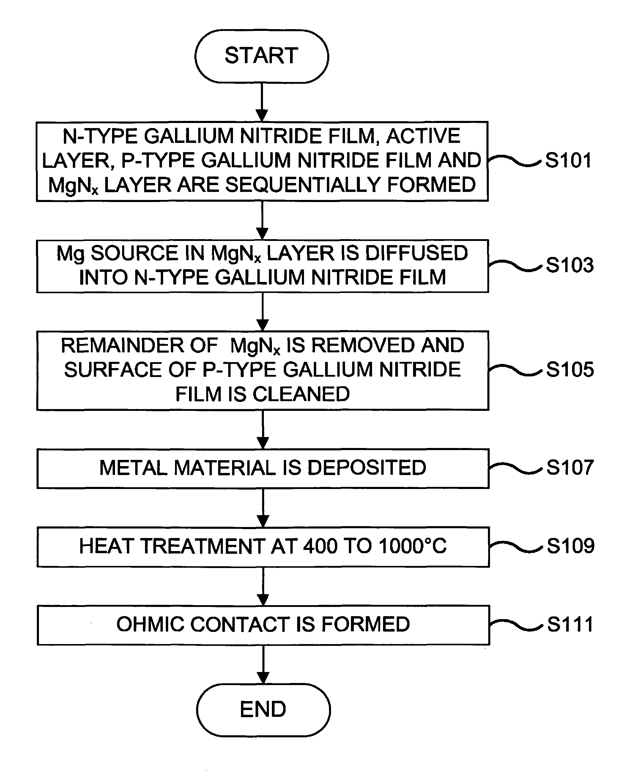
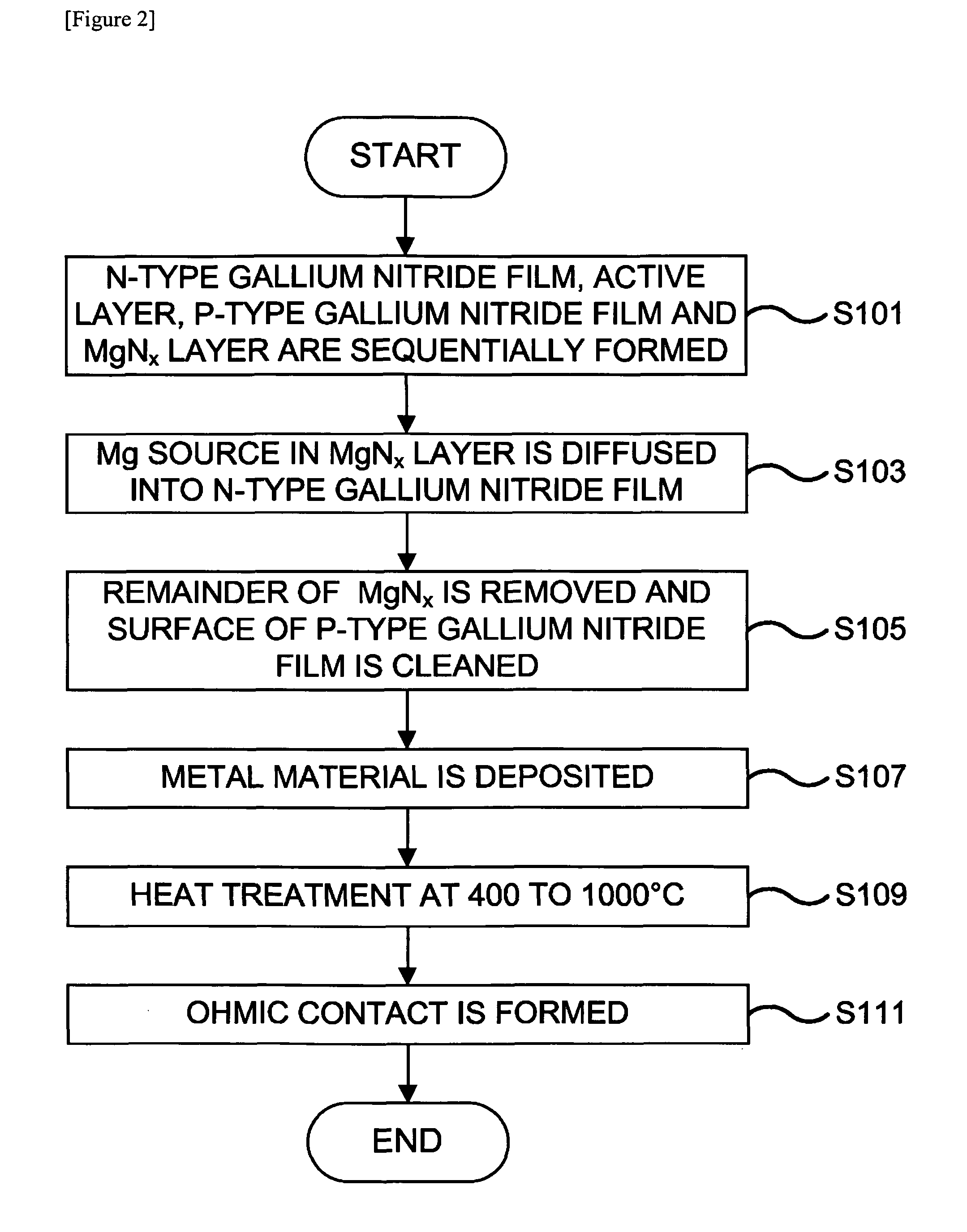
[0040]FIG. 3 is a graph illustrating a result of a depth-profiling of a specimen taken after carrying out the thermal diffusion process in the MOCVD apparatus using an AES (Auger Electron Spectroscopy).

[0041]As shown in FIG. 3, the MgNx layer exists on a surface of the specimen, while the Mg is diffused into the gallium nitride film under the MgNx layer.

[0042]In order to examine a Hall characteristic of the MgNx layer in accordance with the present invention, the Hall characteristic is compared by measuring the Hall characteristics of the p-type gallium nitride prepared in accordance with the conventional art and the p-type gallium nitride prepared in accordance with the present invention.

[0043]A thickness of each of the p-type gallium nitrides is set to be 1 μm, and the Hall characteristic is measured after preparing a Hall sample. A difference in the Hall characteristics of the p-type gallium nitrides in accordance with the conventional art and the present invention are not found ...


PUM

PropertyMeasurementUnit
temperatureaaaaaaaaaa

Abstract

A method for manufacturing a p-type gallium nitride-based (GaN) device is disclosed. In accordance with the method, an Mg in an MgNx layer disposed on p-type gallium nitride is diffused into the p-type gallium nitride by a heat treatment to dope the p-type gallium nitride with the Mg while activating the diffused Mg simultaneously, eliminating a need for an additional heat treatment for the activation and preventing a nitrogen in the p-type gallium nitride from being separated therefrom.

Description

TECHNICAL FIELD[0001]The present invention relates to a method for manufacturing a p-type gallium nitride-based (GaN) device, in particular, to a method for manufacturing a p-type gallium nitride-based device which prevents a vacancy of a nitrogen inside a p-type gallium nitride layer to increase a hole concentration.BACKGROUND ART[0002]A gallium nitride (GaN) compound is a material that emits a light having a wavelength of various regions ranging from a visible light to an ultraviolet ray. The gallium nitride compound is widely used for an electrical device such as a large output / high temperature operation FET (Field Effect Transistor) and a HEMT (High Electron Mobility Transistor) as well as an optical device. Recently, the gallium nitride compound is used in manufacturing a blue LED (light emitting diode).[0003]FIG. 1 is a perspective view illustrating a structure of a gallium nitride-based LED of a conventional art.[0004]Referring to FIG. 1, the LED comprises a sapphire substrat...

Claims


Application Information

Patent Timeline
Patent Type & Authority Patents(United States)
IPC IPC(8): H01L33/00H01L33/32
CPCH01L33/325
Inventor LEE, JONG HEE
Owner THELEDS
Why Eureka
Try Eureka