
Semiconductor apparatus

a technology of semiconductor and apparatus, applied in the direction of semiconductor devices, electrical equipment, basic electric elements, etc., can solve the problems of distortion, deterioration of withstand voltage, leakage current occurrence, etc., to prevent leakage current occurrence, increase the resistance and the switching speed is minimized, the effect of reducing the number of times

Active Publication Date: 2011-06-28
PANASONIC SEMICON SOLUTIONS CO LTD
View PDF2 Cites 0 Cited by
  • Summary
  • Abstract
  • Description
  • Claims
  • Application Information

AI Technical Summary

Benefits of technology

[0017]The invention has been implemented in view of the actual circumstances described above and relates to a semiconductor apparatus having a trench gate. An object of the invention is to provide a semiconductor apparatus which prevents stress occurring by metal wiring etc. from directly acting on a trench and has high reliability with respect to a withstand voltage and leakage characteristics.
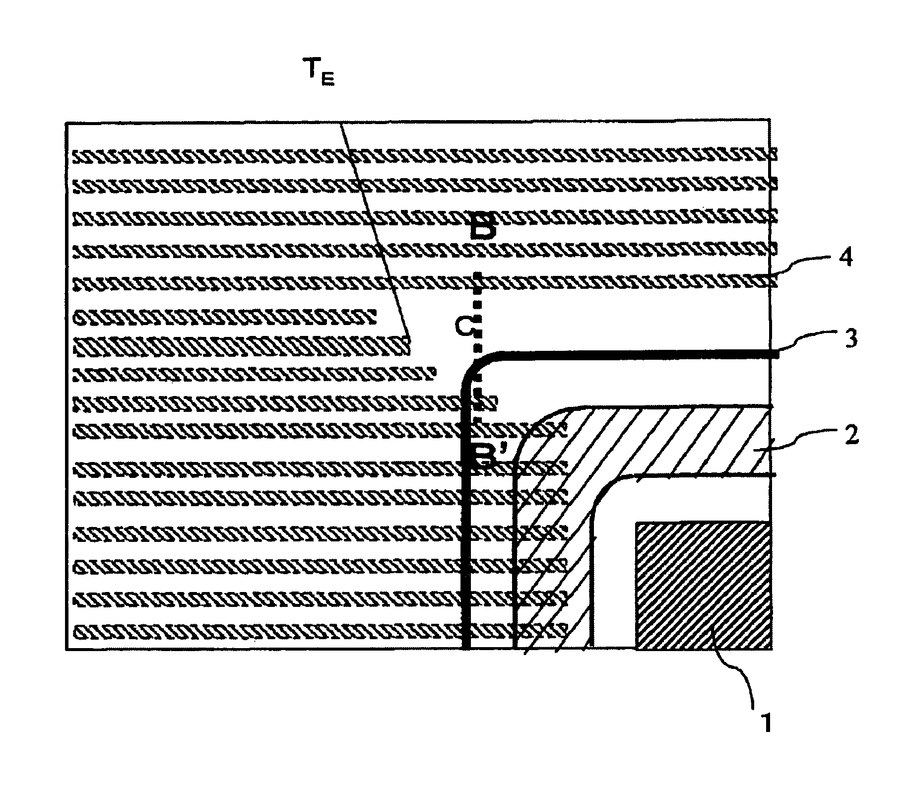
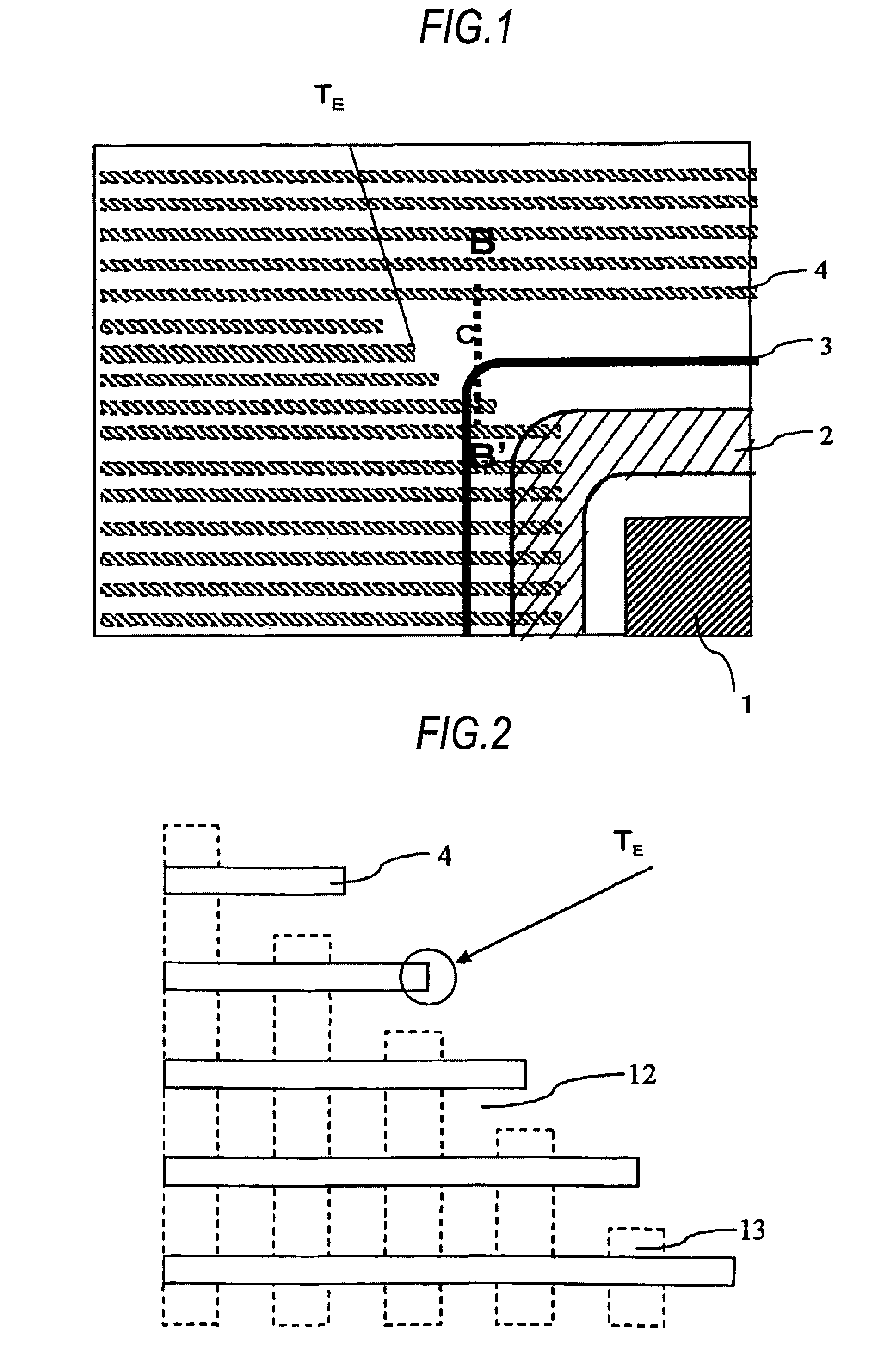
[0018]In order to solve the problems described above, the semiconductor apparatus is formed so that the end of a trench is not present at a corner portion of a source contact opening part where stress by an (interlayer) insulating film or metal wiring concentrates. As a result, the stress is not applied to the trench and the trench is not distorted structurally. Also, the trench end in which a sub-trench tends to be generated is constructed so as not to be near to the corner portion of the source contact opening part. That is reason why the portion with insufficient oxide film is not used as a channel region. Therefore, according to this configuration, deterioration of a withstand voltage and leakage characteristics can be prevented. A distance between the source contact opening part and the trench gate is preferably 1 μm or longer. In this condition, deterioration of a withstand voltage can be prevented.
[0019]Also, in the case of adjusting a length of a trench line, a termination part of the trench line is disposed from the corner portion of the source contact opening part in an uniform distance (1 μm). By this configuration, a decrease in a channel width per unit area can be minimized so as to prevent an excessive increase in on resistance.

Problems solved by technology

Thus, there is a problem that deterioration of a withstanding voltage at the sub-trench is not avoidable.
However, in recent years, demands on high current increase and a film thickness of metal wiring as an electrode formed on a surface of a chip constructing this semiconductor apparatus is thick relative to a trench size.
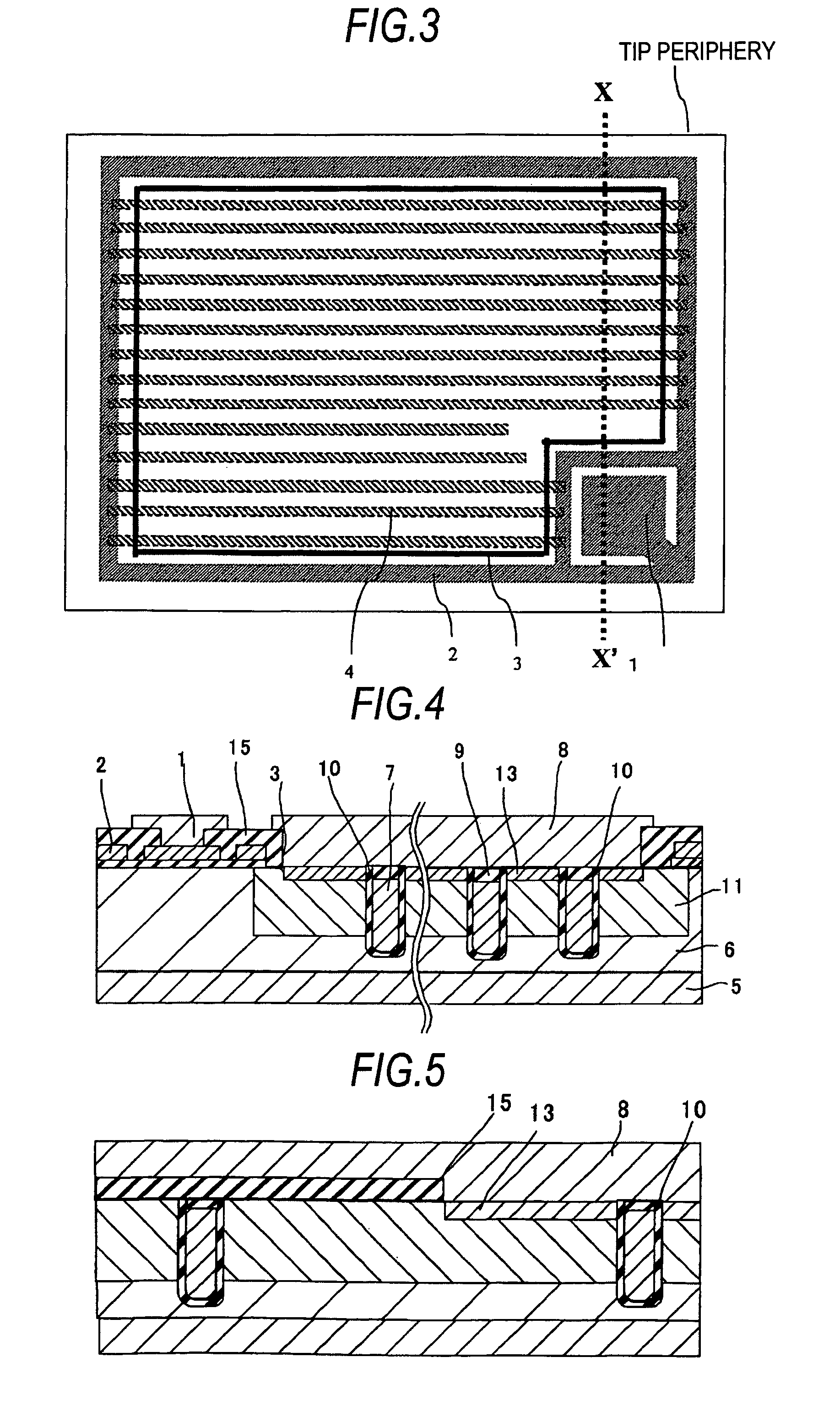
First, an N-type MOSFET having a conventional stripe-shaped trench gate is explained with reference to FIGS. 9 to 12 as one example of a semiconductor apparatus in order to manifest the problem. FIG. 9 is a top diagram of this N-type MOSFET and a sectional diagram of X-X′ of FIG. 9 is shown in FIG. 10. A plurality of trench lines are formed on a semiconductor layer and termination parts of the trench lines are directly connected to gate peripheral wiring. An N-type diffusion region constructing a source region is formed in an epitaxial layer of both ends so as to abut on the trench lines. Also, the opening end of a region in which an N-type diffusion layer constructing a source region 13 is electrically connected to metal wiring constructing a source electrode (pad) 8, that is, a source contact opening part 3 is disposed on trench lines (4) as shown in FIG. 9. As shown in FIG. 9, in a region of a corner part α of the opening end of a source electrode, a corner portion of a source contact opening part is formed on terminations of the trench lines (4) because of placement of a pattern. At this time, stress by the thick metal wiring constructing the source electrode 8 concentrates in the vicinity of this corner and causes distortion in a trench structure located in a lower part (FIG. 10 is a main enlarged explanatory diagram corresponding to a section of A-A of FIG. 11 (a main enlarged diagram of FIG. 9)). Also, formation of the corner portion of the source contact opening part 3 on the terminations of the trenches 4 means that the edge of an insulating film 15 is also positioned on this trench and when the trench end is present in a lower part of the edge of the insulating film 15, a channel of this transistor is formed along an outer wall of the trench. As a result of this, when distortion occurs in the trench, distortion also occurs in the channel formed along the outer wall of the trench and problems of an increase in a leakage current and a decrease in a withstand voltage between a drain and a source might arise.
Also, in the leakage current, the problem of the leakage current resulting from the trench distortion was serious in a body region as well as the source region.
This region is the cause of a problem that stress by metal wiring etc. constructing a source electrode concentrates and distorts a trench structure and a withstand voltage and leakage characteristics are deteriorated.
This problem becomes particularly serious as a trench becomes finer and a film thickness of the metal wiring constructing the source electrode becomes thicker with respect to a trench width.
Now the occurrence of distortion in the vicinity of the trench depending on whether or not to abut on the metal wiring with a thick film thickness becomes a serious problem.
In the case of thermal oxidation of an inner wall of the trench, insufficient supply of oxygen makes a film thickness of a silicon oxide film thin.
As a result, when a high electric field is applied to this portion, deterioration of a withstand voltage occurs.
Furthermore, an insulating film formed on gate wiring causes stress distortion to a trench in a connection part to the gate wiring of a peripheral edge part of a chip.

Method used


Image

  • Semiconductor apparatus
  • Semiconductor apparatus
  • Semiconductor apparatus

Examples


second embodiment

[0064]Next, a second embodiment of the invention is described.

[0065]The first embodiment is constructed so that the termination parts of the trenches are distant from the corner portion of the source contact opening part 3 by the predetermined distance (1 μm) or longer as shown in FIG. 2. Instead, the present embodiment is characterized in that termination parts of trenches are distant from a corner portion C by an equal distance (1 μm) as shown in FIGS. 7A and 7B. FIG. 7B is a main enlarged diagram of FIG. 7A. Since a source region 13 made of an N-type diffusion layer is also formed in a direction orthogonal to a trench 4 herein, it is easy to form the source region 13 in a state of avoiding the end of the trench. As a result a decrease in a channel width per unit area is minimized and an excessive increase in on resistance is prevented.

[0066]In this second embodiment, with respect to a trench having a possibility of being positioned within 1 μm from the corner portion of the sourc...

third embodiment

[0069]Next, a third embodiment of the invention will be described.

[0070]In the second embodiment, termination positions of the trenches are gradually changed so that the termination parts of the trenches are distant from the corner portion of the source contact opening part 3 by the equal distance (1 μm) as shown in FIGS. 7A and 7B. In addition to this feature, in this third embodiment, a coupling trench 14 for coupling adjacent trenches in the vicinity of the trench ends are disposed as shown in FIGS. 8A and 8B. In addition, a source region 13 is not disposed in the vicinity of the coupling trench 14.

[0071]According to this configuration, by directly connecting the adjacent trenches by the coupling trench 14, an increase in gate resistance is prevented and a switching speed is reduced.

[0072]Also, as the source region is not disposed in the vicinity of the coupling trench, performance of the MOSFET is stabilized. This stabilization is a result of formation of channels so as not to b...


PUM


Abstract

The present invention provides a semiconductor apparatus having high reliability with respect to a withstand voltage, leakage characteristics, etc. by disposing a structure of preventing stress occurring by metal wiring from directly acting on a trench relating to the semiconductor apparatus having a trench gate. The semiconductor apparatus of the invention includes a semiconductor substrate including a semiconductor layer having a predetermined impurity concentration, a trench gate formed in the semiconductor layer by filling a stripe-shaped trench by a conductor layer on which surface and interface a gate oxide film is formed, an insulating film covering a surface of the semiconductor layer and having a source contact opening, a source region formed in the semiconductor layer, a source electrode formed on the surface of the semiconductor layer so as to electrically connect to the source region through the source contact opening, a gate peripheral wiring connected to the trench gate at a peripheral edge part of the trench gate, a gate electrode separately formed from the source electrode, formed above the surface of the semiconductor layer and connected to the gate peripheral wiring and a drain electrode formed on an surface of the semiconductor substrate opposite to the surface of the semiconductor layer, wherein the trench gate is formed so as to avoid a corner portion of the source contact opening of the source electrode.

Description

BACKGROUND OF THE INVENTION[0001]The present invention relates to a semiconductor apparatus, and particularly to a semiconductor apparatus such as an insulated gate transistor having a trench structure.[0002]In recent years, as a speedup, high functionalization and low power consumption in electronic equipment such as a mobile telephone are required, a speedup and low power consumption are also desired in a semiconductor apparatus installed in the electronic equipment. Generally, a transistor used in a DC-DC converter and a load switch, etc. with small on resistance is required in order to cope with the speedup and low power consumption. As a method to reduce the on resistance of the transistor, miniaturizing an individual device and increasing a density of a transistor placed per unit area is given. Concrete method is a miniaturization of a trench in a vertical MOSFET with a gate electrode formed in the trench. In this method, the trenches in which transistors are formed are placed...

Claims


Application Information

Patent Timeline
Patent Type & Authority Patents(United States)
IPC IPC(8): H01L29/66
CPCH01L29/4238H01L29/7813H01L29/7811H01L29/66734H01L29/4236
Inventor KUMEKAWA, TATSUMIHAMADA, MITSUHIROMIZOKUCHI, SHUJI
Owner PANASONIC SEMICON SOLUTIONS CO LTD
Learn More