
Self-gating synchronizer

a synchronizer and self-gating technology, applied in the field ofsignal synchronization, can solve the problems of metastability, the failure mode of most digital systems, and the unpredictable system behavior of the synchronous digital system, so as to reduce power consumption and silicon area, and reduce the latency of synchronization. , the effect of speed increas

Inactive Publication Date: 2011-07-12
APPLE INC
View PDF7 Cites 15 Cited by
  • Summary
  • Abstract
  • Description
  • Claims
  • Application Information

AI Technical Summary

Benefits of technology

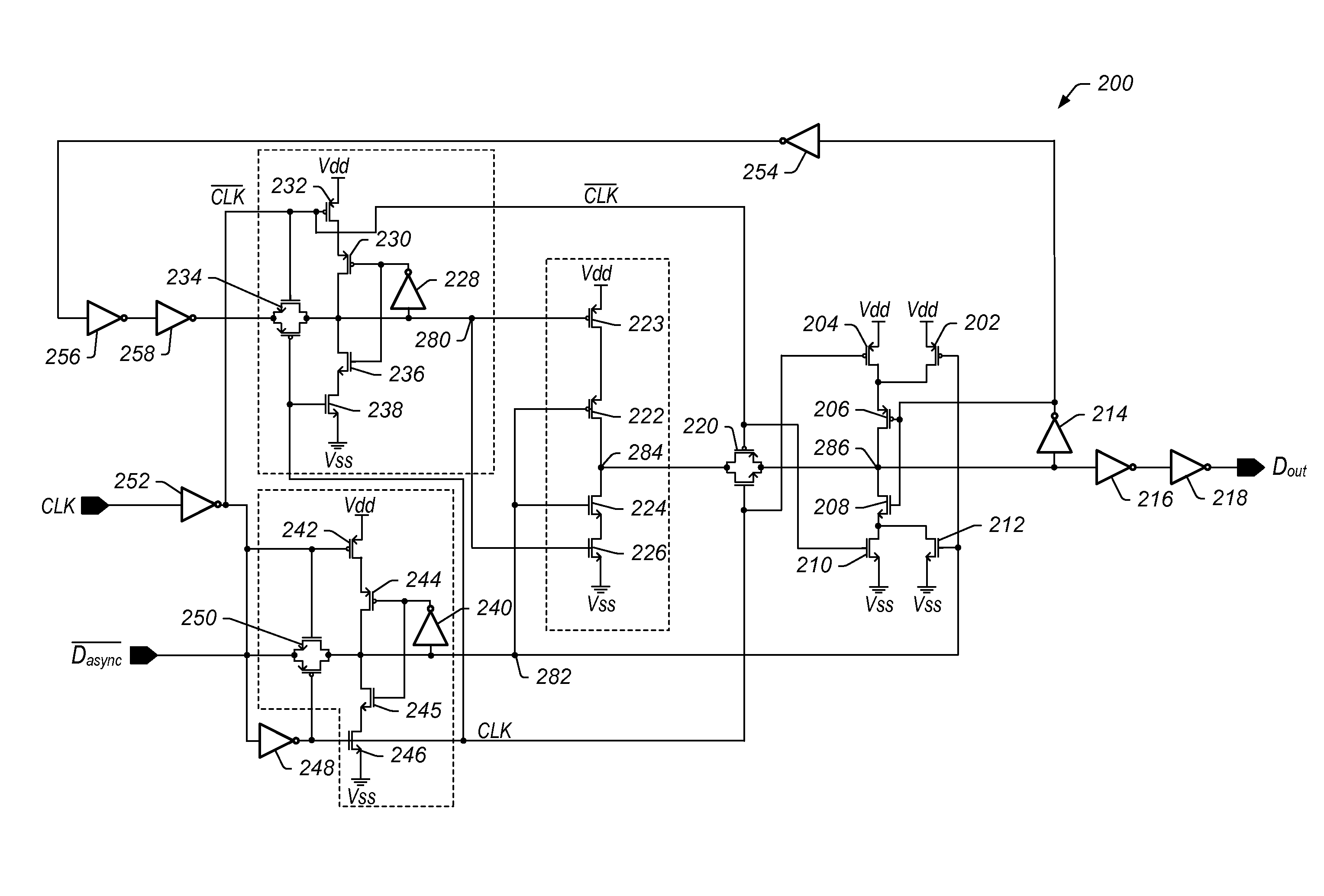
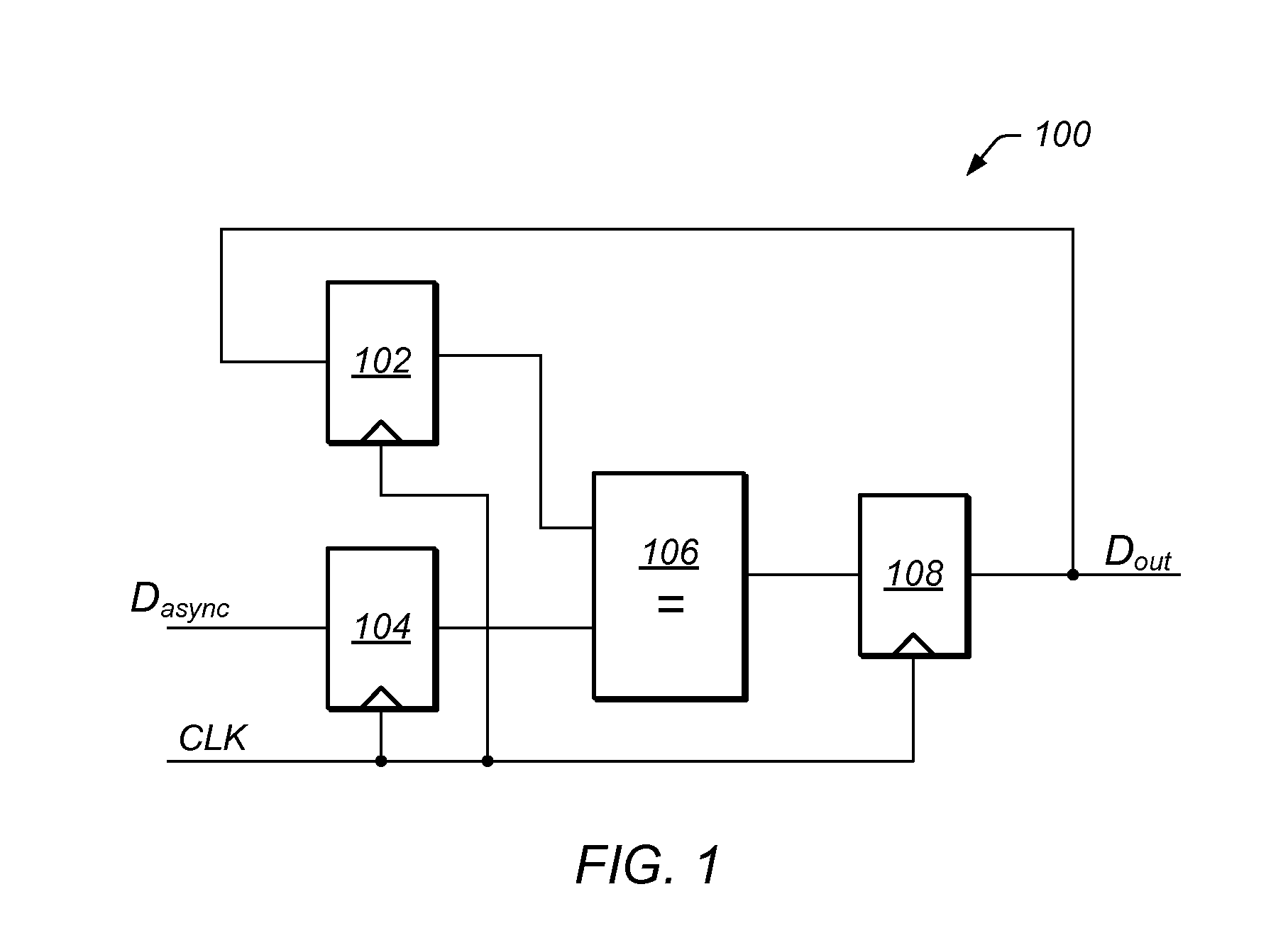
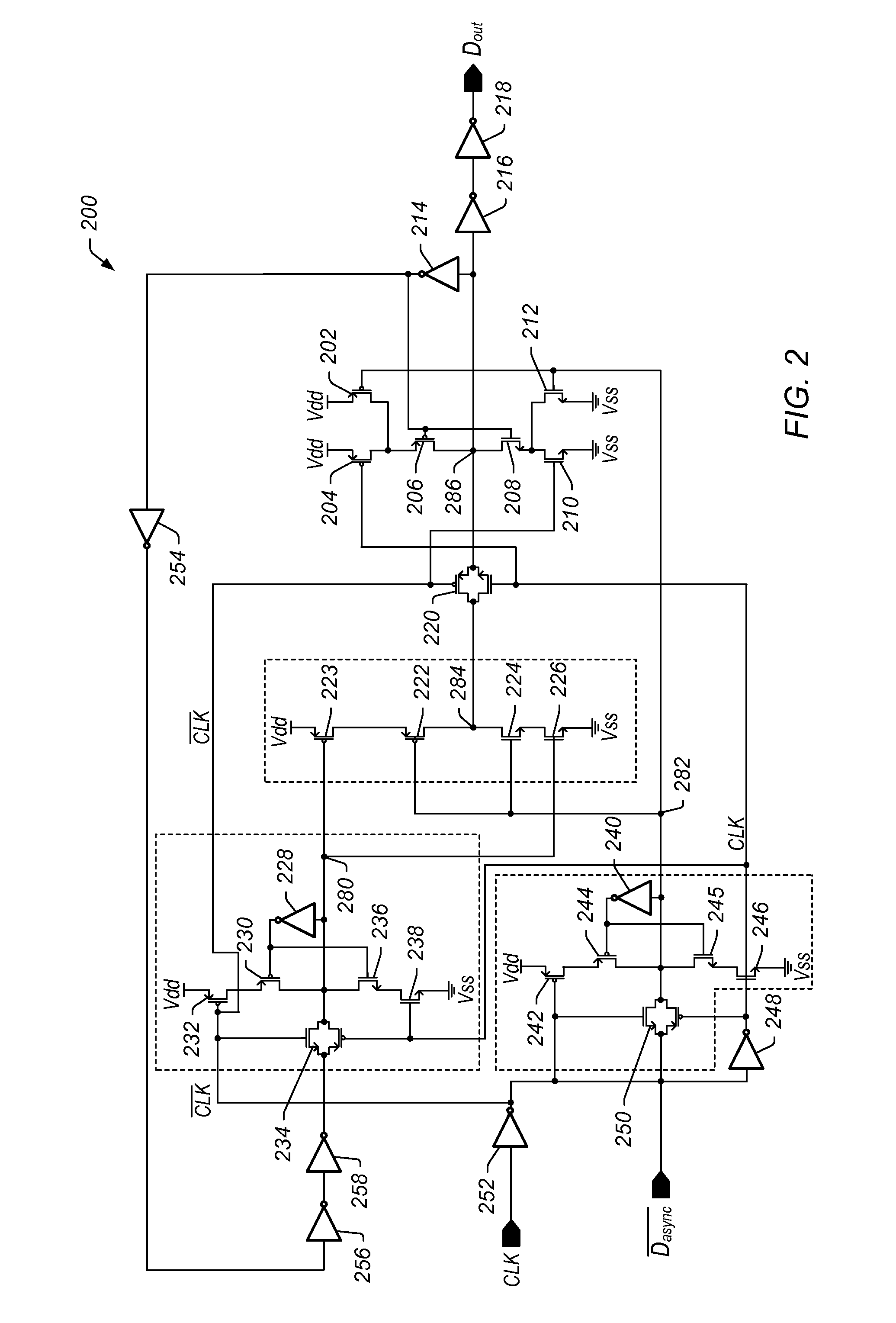
In one set of embodiments, a synchronizer circuit may be used to transfer data from a source clock domain to a target clock domain. A first latch in the target clock domain may capture a data value corresponding to current data from the source clock domain. Under certain conditions, the first latch may enter into a metastable state (i.e. an undefined logic state, or logically undefined state). A second latch may store a previous value (e.g. a most recent previous value) corresponding to data that has been transferred from the source clock domain to the target clock domain. The stored previous value may remain stable. The respective values output by the two latches may be compared by a detection circuit, and a value derived from the output value of the first latch and corresponding to the current data may be written to an output latch if the current data differs from the stored previous value. The detection circuit may also operate to provide a definite logical value even if the first latch is in a metastable state.
When the sampled current data is in a metastable state, a PMOS transistor and an NMOS transistor, within the detection circuit and driven by the first latch, may both be partially conducting. However, an upper PMOS transistor and a lower NMOS transistor, also within the detection circuit but driven by the second latch, may either have a pull-up or pull-down enabled but not both, resulting in the output (slave) latch driven to a clearly defined logical state. The output latch may be implemented with a two-branch keeper operating to prevent contention on the input of the output latch during a write operation into the output latch, which would occur when the sampled current data indicated that the current value differed from the previous value. In one set of embodiments, the two-branch keeper configuration may also be designed to prevent the input of the output latch from floating when the sampled current data indicates that current value is the same as the previous value. The propagation of the metastable state may therefore be blocked, resulting in the logic stage of the output of the synchronizer circuit residing at either a clear logic “1” state or a clear logic “0” state even when the output of the sampling latch resides in a metastable state.
At least one advantage of various embodiments of the synchronizer circuits disclosed herein is the elimination of the need for high-gain latches, which reduces power consumption and silicon area. Embodiments of the synchronizer circuits presented herein may also replace any multiple-stage synchronizer circuit with circuits featuring no more than two stages. The latency of synchronization may be thereby reduced, producing a noticeable gain in speed.

Problems solved by technology

While running a digital system using a system clock may theoretically provide stable and predictable operation, there are certain conditions under which the operation of a synchronous digital system may yield unpredictable results.
This can result in various portions of the system, or even the entire system—depending on the signal path where the metastable condition first occurs—to enter and remain in an undefined state, producing unpredictable system behavior.
Metastability is therefore considered a failure mode in most digital systems.
However, careful design techniques can often reduce failures caused by metastability.
In digital circuits, latches and flip-flops are often susceptible to metastability.
First, if the target clock has a different frequency than the clock used in operating the source flip-flop, the setup and hold time of the target flip-flop can be violated.
Second, when the target and source clock have the same frequency, a phase alignment can cause the data to arrive at the target flip-flop during its setup and hold time.
These conditions can result from fixed overhead or variations in logic delay times on the worst case path between the two flip flops, or variations in clock arrival times (clock skew), or yet other causes.
In general, to meet the required mean time to failure (MTTF), multiple stage flip-flops may be needed which increases the overall latency.
In addition, high-gain latches can use a significant amount of power, and are prone to leakage current as well.

Method used


Image

  • Self-gating synchronizer
  • Self-gating synchronizer
  • Self-gating synchronizer

Examples


Embodiment Construction

As described herein, for ease of reference, a data signal and / or a data value is said to be metastable, or in a metastable state when its value is undefined in terms of the expected logic values in a digital system. Such a state is also referenced as a logically undefined state, indicating for example that a voltage value representing the data value does not correspond to a logically defined state such as logic ‘0’ or logic ‘1’. Accordingly, the behavior of such signal could potentially cause a circuit or logic block within a circuit / system—to which the data signal / value is provided—to also enter a metastable state, or logically undefined state, thereby propagating the metastable state within the system. For example, in a synchronous circuit operated according to a given clock signal, a data signal or data value provided to a given latch may transition at the same time, or very close to the same time as the clock signal / value on which the data value is gated by the given latch. This...


PUM


Abstract

A synchronizer circuit for transferring data from a source clock domain to a target clock domain. A first latch in the target clock domain may capture a data value corresponding to current data received from the source clock domain. Under certain conditions, the first latch may enter into a metastable, or undefined logic state. A second latch may remain stable, and store a previous value corresponding to data that has most recently been transferred from the source clock domain to the target clock domain. The respective values output by the two latches may be compared by a detection circuit, and a value derived from the output value of the first latch and corresponding to the current data may be written to an output latch if the current data differs from the stored previous value. The detection circuit may also provide a defined logical value to the output latch even if the first latch is in a metastable state.

Description

BACKGROUND1. Field of the InventionThis invention is related to the field of signal synchronization, more specifically to preventing propagation of metastable signals.2. Description of the Related ArtMost circuits in today's digital systems are synchronous circuits. A synchronous circuit or system is characterized by a clock signal that is used to control operation of the system by synchronizing the various components / circuit elements of the system / circuit, including the operation of the system / circuit's memory / storage elements and latches. Ideally, in a synchronous system, every change in the respective logical levels of the system's storage components is simultaneous, following the level changes of the clock signal. The expectation is for the input signal into each storage element to have reached its final value before the next change in the clock signal occurs, to obtain a deterministic, predictable behavior of the system.While running a digital system using a system clock may th...

Claims


Application Information

Patent Timeline
IPC IPC(8): H03K19/00
CPCH03K5/135H04L7/02H04L7/0045
Inventor TANG, BOKLASS, EDGARDO F.
Owner APPLE INC
Learn More