Color filter structure and display device using the color filter, and manufacturing method thereof

a color filter and structure technology, applied in the field of color filter structure and display device using the color filter, can solve the problems of not giving any consideration for simplifying a manufacturing process from aspects such as actual cost and yield or the like, and the quality degradation of display colors in a whole screen area, so as to reduce the difference in the coloring effect of light, reduce the cell gap, and reduce the effect of cell gap

Inactive Publication Date: 2011-08-09
INNOLUX CORP
View PDF7 Cites 2 Cited by
  • Summary
  • Abstract
  • Description
  • Claims
  • Application Information

AI Technical Summary

Benefits of technology

[0026]By doing this, the stepped layer is eliminated, and the individual color portion of a respective one of the reflection region and the transmission region is formed in accordance with the ink jet technique, so that the whole manufacturing process is simplified. In this case as well, by the presence of the rib, the dropping material is dammed from outflow to the outside of the rib, and thus, there is no need for so high precision in a dropping operation. In addition, similarly, the color filter structure is formed in a shape such that it is incorporated in the composite layer in the rear substrate, and thus, no alignment problem occurs. Advantageous effects specific to these aspects are that a comparatively simple structure can be employed because the stepped layer is not formed and that the second rib is formed at the same height as that of the first rib, thus making it possible to simplify a configuration of a photo mask for forming these ribs.
[0027]In these fifth and sixth aspects, it is desirable that the first and second color portion be defined in their respective thickness and / or material so as to exhibit a coloring effect that the first color portion is lower than the second color portion. In this manner, it becomes possible to reduce a difference in coloring effect of light handled in a respective one of the reflection region and the transparent region, and then, achieve uniform color reproducibility in pixels. In addition, it is preferable that the first color portion should have a surface that is higher than that of the second color portion. In this manner, it becomes possible to reduce a cell gap in the reflection region more significantly than that in the transmission region. In addition, it becomes possible to reduce an optical path difference between the reflection light and the transmission light in the display panel. That is, the reflection region has a forward path for the light incident from the outside of the front substrate to arrival at the reflection layer and a backward path for light reflection from the reflection layer to exit to the outside of the front substrate. Logically, the reflection region exhibits an optical path that is as twice in length as the transmission light in the transmission region. Thus, the cell gap in the reflection region is reduced, thereby making it possible to reduce the lengths of the forward path and the backward path so as to equal to a optical path for transmission light.
[0028]In addition, in these fifth and sixth aspects as well, a reflection portion formed in a lower layer of the first color portion in the reflection region can be provided. At least a part of a base portion defining a surface shape of the reflection portion can be formed simultaneously or integrally with the first rib and / or the second rib. A light transmission conductive layer that extends over a surface of the color layer can be further provided; the reflection portion can have a light reflection conductive film that extends over a main face thereof and extends up to a top face of the rib, and the light reflection conductive film can be connected to the light transmission conductive layer in the top face. Advantages relating to these aspects are attained as described above.
[0029]In each of the above-described aspects, it is convenient if the rib is formed of a light interruption material, because the rib functions as a so-called black matrix. In particular, in the case where a second rib is formed, there is attained an advantage that the second rib can hide the behavior of unnecessary light can be hidden, the unnecessary light having a possibility of occurring at a junction portion between the reflection region and the transmission region. In addition, if the base portion has an irregular surface for exhibiting light scattering property, there is no need for additionally providing a light scattering layer. Moreover, such no need is convenient because scattering can be applied only to reflection light.
[0030]According to a preferred aspect of the manufacturing method, as in the first aspect, each region defined by the first rib and the second rib in which the light transmission material is dropped is disposed linearly in a main face of the composite layer to form a plurality of line regions, and, in the third step, at least one ink jet head, an ejection portion of which is opposed to the line region and is moved along a longitudinal extending direction of the line region, carries out dropping of the light transmission material for each of the line regions. In addition, as in the first and third aspects, each region defined by the rib in which the light coloring material is dropped is disposed linearly in a main face of the composite layer to form a plurality of line regions, and, in the fourth step, at least one ink jet head, an ejection portion of which is opposed to the line region and is moved along a longitudinal extending direction of the line region, carried out dropping of the light coloring material for each of the line regions. Further, as in the fifth aspect, in the third step, the each reflection region is disposed linearly in a main face of the substrate to form a plurality of line regions; at least one ink jet head, an ejection portion of which is opposed to the line region and is moved along a longitudinal extending direction of the line region, carries out dropping of a light coloring material for the first color portion for each of the line regions, and / or the each transmission region is disposed linearly in a main face of the substrate to form a plurality of line regions, and at least one ink jet head, an ejection portion of which is opposed to the line region and is moved along a longitudinal extending direction of the line region, carries out dropping of a light coloring material for the second color portion for each of the line regions. These aspects are featured in that the dropping regions are linearly arranged, and displacement of an ink jet head is carried out by means of simple control, thereby leading to improved effectiveness of the manufacturing steps.
[0031]A still another aspect of the present invention is directed to a display device using a color filter structure derived from each of the above described aspects, wherein the color filter structure is eliminated from the front substrate, and the reflection region modulates light incident into the display panel from an outside of the front substrate in a reflection mode for each pixel, and a region other than the reflection region in a pixel region modulates light incident into the display panel from an outside of the rear substrate in a transmission mode, thereby forming a color display image. In this manner, a display device having the above described various advantages is provided. In particular, this aspect is suitable to a transflective type liquid crystal display device.

Problems solved by technology

This difference is caused by the fact that light from a backlight system and external light respectively having different optical paths from each other are colored in the same manner, and this causes quality degradation of display colors in a whole screen area.
In the above described conventional art, while a structure for obtaining a color balance in a pixel is primarily proposed, there is no specific disclosure of how to efficiently manufacture a color filter having such a structure.
Additionally, in spite of the fact that the manufacturing steps has become complicated by complicating a pixel structure in order to enable the color balancing, consideration for simplifying a manufacturing process from aspects such as actual cost and yields or the like is not given at all.
However, the manufacturing in accordance with the lithography technique requires a number of steps and photo masks, and is disadvantageous in simplification of the whole manufacturing process.
This increases a burden in development and manufacturing.

Method used


Image

  • Color filter structure and display device using the color filter, and manufacturing method thereof
  • Color filter structure and display device using the color filter, and manufacturing method thereof
  • Color filter structure and display device using the color filter, and manufacturing method thereof

Examples


first embodiment

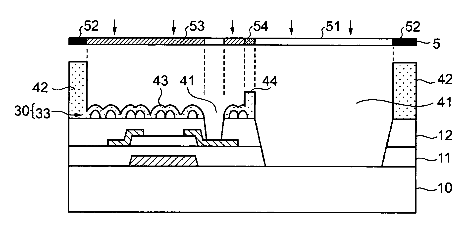
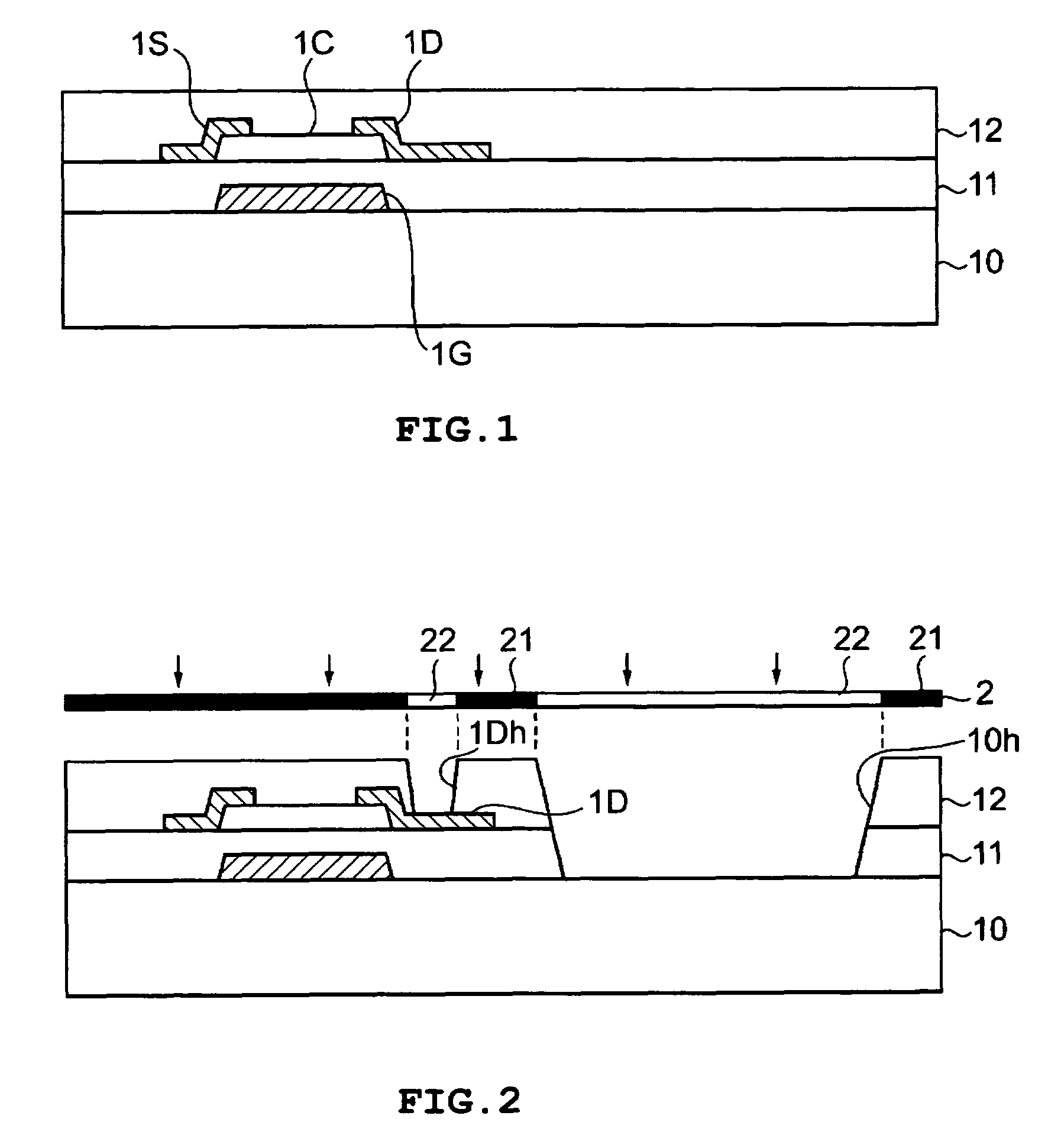
[0056]In FIG. 1, there is shown a structure of a composite layer including a TFT (thin film transistor) that is a pixel drive element of a liquid crystal display device. In order to form this structure, first, a glass substrate 10 serving as a substrate is prepared. After required treatment such as washing has been carried out, a metal material such as aluminum is deposited on the substrate, and is patterned to form a gate electrode 1G of the TFT and a gate bus line (not shown) connected thereto. The gate electrode 1G is formed here on a pixel-by-pixel basis. After these gate-associated portions have been formed, an electrical insulation material such as SiNx is deposited fully on the substrate to form a first insulation layer 11. On the insulation layer 11, amorphous silicon (a-Si) serving as a semiconductor material and phosphor (P)-doped amorphous silicon each are deposited in order and are patterned to form a semiconductor layer 1C. The semiconductor layer 1C is formed in a shap...

second embodiment

[0085]Now, another embodiment of the present invention will be described with reference to FIG. 12 to FIG. 15.

[0086]In the present embodiment, masking and exposure treatments as shown in FIG. 12 are carried out after the steps corresponding to FIG. 1 to FIG. 4 in the above described embodiment have been carried out similarly in general. While a mask 5A shown in FIG. 12 is defined as a half-tone mask, this mask is patterned according to five types of portions in this embodiment. A difference from the case of FIG. 5 is that a fifth portion 55 having a transmission rate between a fourth portion 54 and a second portion 52 (about 10% in this embodiment) is provided between a second portion 52 and a third portion 53. The fifth portion 55 is indicated by a white dot on a black base in the figure. In addition, although it cannot be read from FIG. 12, an organic material 4 deposited before masking is defined to be higher than that shown in FIG. 4. This is because a photo spacer described lat...

third embodiment

[0092]Now, still another embodiment of the present invention will be described with reference to FIG. 16 and FIG. 17.

[0093]In the present embodiment, after the steps corresponding to FIG. 1 to FIG. 4 in the first embodiment have been carried out similarly in general, masking and exposure treatments as shown in FIG. 16 are carried out. Although a mask 5B shown in FIG. 16 is defined as a half-tone mask, this mask is patterned according to three types of portions in this embodiment. A difference from the case of FIG. 5 is that a fourth portion 54 is not provided and that only first to third portions 51 to 53 are provided.

[0094]After exposure treatment has been carried out using such a photo mask 5B, when developing treatment and fixing treatment are done, there are formed: a portion 41 corresponding to a first portion 51 of the photo mask 5B; a portion 42 corresponding to a portion 52 thereof; and a portion 43 corresponding to a portion 53 thereof. The portion 41 is provided as a porti...


PUM

PropertyMeasurementUnit
heightaaaaaaaaaa
light transmissionaaaaaaaaaa
coloraaaaaaaaaa

Abstract

A color filter being precisely and easily manufactured while solving an alignment problem is provided. Further, a method for manufacturing a color filter structure formed in a display panel that has front and rear substrates opposed to each other is provided. This method is provided with: a first step of forming a composite layer (11, 12, 1G, 1C, 1S, 1D) that includes a pixel drive element in a rear substrate 10; a second step of patterning a first rib 42 along a boundary of a pixel region on or above the composite layer and a second rib 44 arranged in the pixel area, the second rib having a height that is smaller than that of the first rib 42 in accordance with a photolithography technique; a third step of dropping a light transmission material in a reflection region Pr defined by the first rib 42 and the second rib 44 and forming a stepped layer 7 in accordance with an ink jet technique; and a fourth step of, after the stepped layer 7 has been formed, dropping a light coloring material 9 in a region defined by the first rib 42 and forming a color layer in accordance with an ink jet technique.

Description

[0001]This application claims the benefit of Japan Application Ser. No. 2005-227724, filed Aug. 5, 2005.BACKGROUND OF THE INVENTION[0002]1. Field of the Invention[0003]The present invention relates to a display device using a color filter structure and a manufacturing method of such display device. In particular, the present invention relates to a color filter structure suitable for a transflective type liquid crystal display device equipped with a transmission region and a reflection region on a pixel-by-pixel basis or by a predetermined unit display region, as well as to a manufacturing method of such a color filter structure.[0004]2. Description of the Related Art[0005]Conventionally, a color filter has been well known that handles: first light for forming a unidirectional optical path, such that incident light from one main face side of the color filter is transmitted through the filter only once to be colored and guided to the other main face side; and second light for forming ...

Claims


Application Information

Patent Timeline
Patent Type & Authority Patents(United States)
IPC IPC(8): G02B5/20G02F1/1335
CPCG02F1/133555G02F1/133371G02F1/133514G02F1/133516G02F2001/136222G02F2203/09G02F1/136222
Inventor HAMAWAKI, YOSHIHIKOHATTA, YASHIHISAMATSUSHITA, YASUHIRO
Owner INNOLUX CORP
Why Eureka
Try Eureka