Method of improving nanotopography of surface of wafer and wire saw apparatus
a technology of wire saw and surface, which is applied in the field of improving the nanotopography of the surface of the wafer and wire saw apparatus, can solve the problems of nanotopography sensory test rejection, the size of the surface waviness component called a “nanotopography” is a problem, and the numerical value judgment of nanotopography, so as to improve the straightness of the feed of the work feed table, improve the surface nanotopography, and eliminate the effect of cutting
- Summary
- Abstract
- Description
- Claims
- Application Information
AI Technical Summary
Benefits of technology
Problems solved by technology
Method used
Image
Examples
example 1
Comparative Example 1
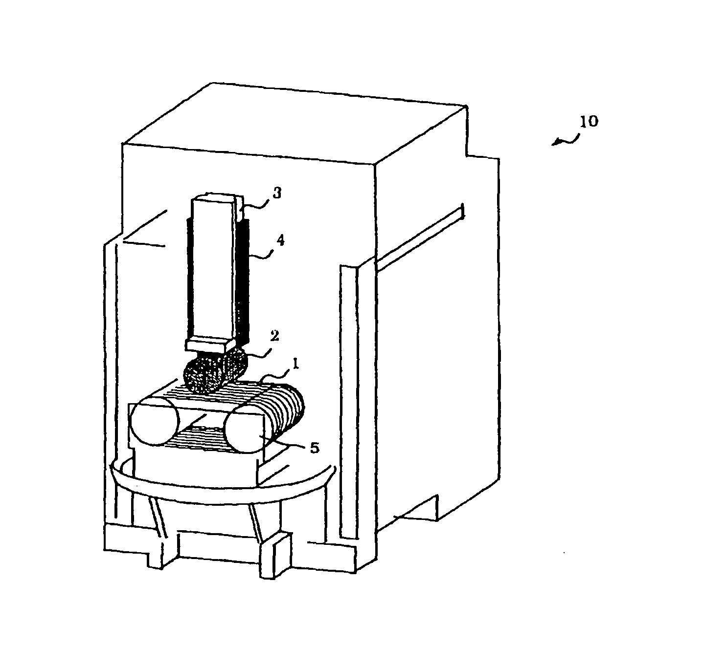
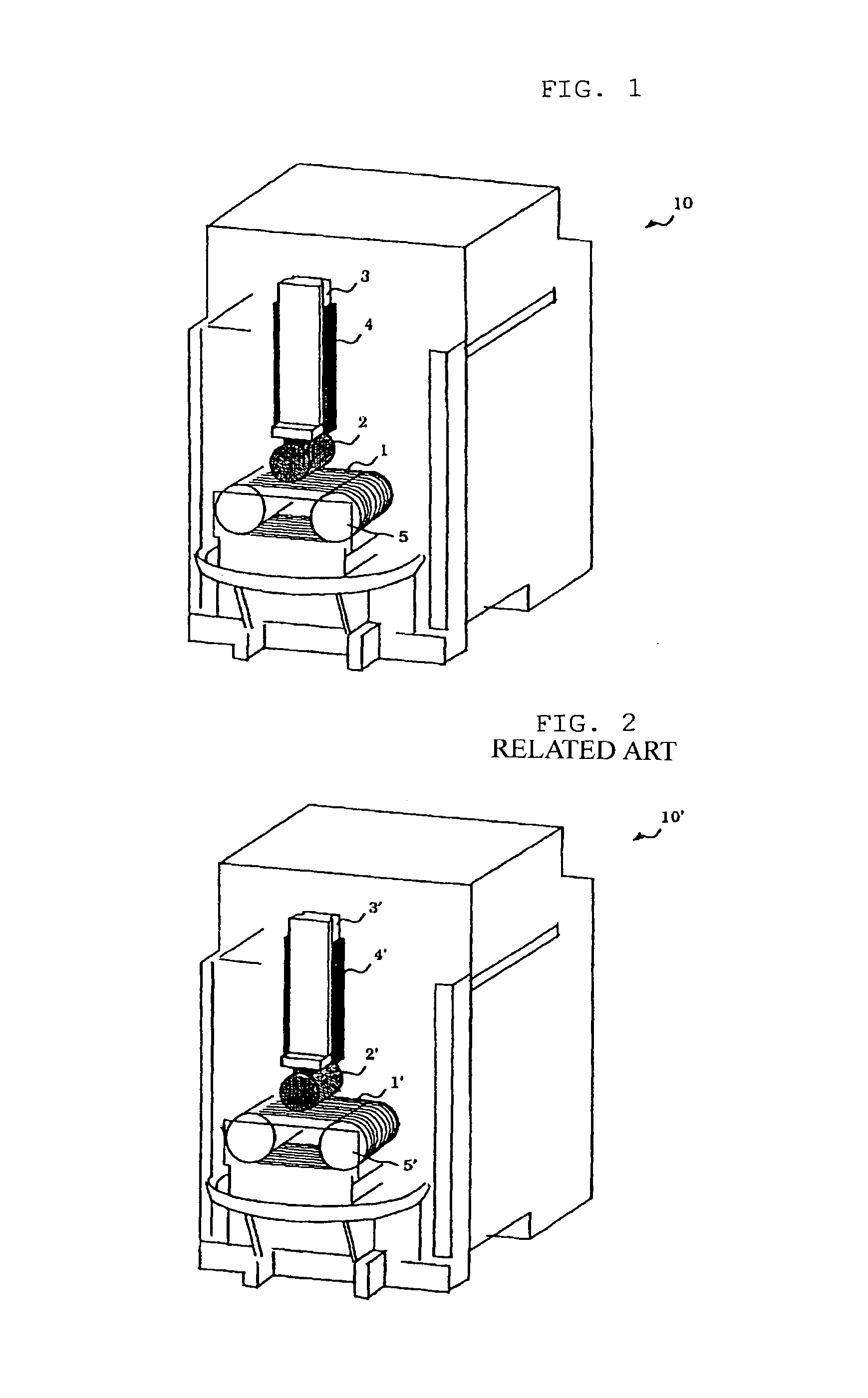
[0046]In the wire saw apparatus shown in FIG. 1, intervals of attachment holes which are used to attach an LM guide to the wire saw apparatus by using the bolts and tightening torque of bolts were respectively adjusted from 100 mm and 60 Nm (Comparative Example 1) to 75 mm and 40 Nm (Example 1) like the above-explained simulation. Further, straightness of feed of the work feed table was measured by the same method as above.
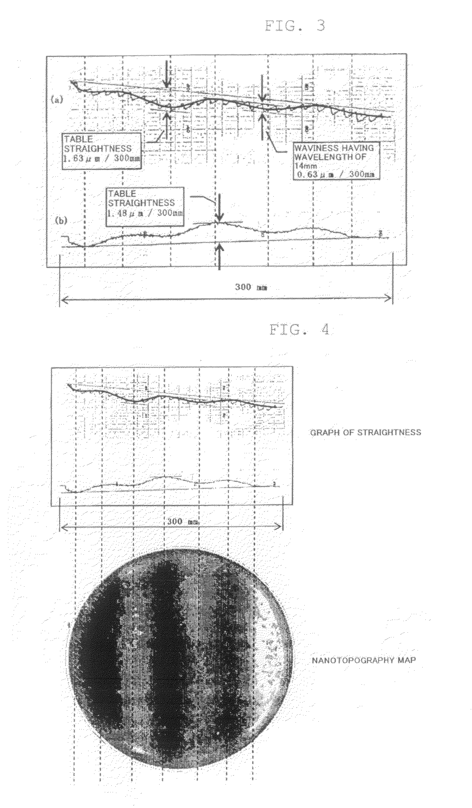
[0047]As a result, while straightness of feed of the work feed table was 1.48 μm / 300 mm and a component having a wavelength of approximately 100 mm was 1.48 μm in terms of a PV value in Comparative Example 1, straightness of feed of the work feed table was 0.92 μm / 300 mm and a component having a wavelength of approximately 100 mm was 0.92 μm in terms of the PV value in Example 1 as shown in FIG. 6, thereby providing the wire saw apparatus having the greatly improved straightness of feed of the work feed table. Based on a result depicted in FIG...
example 2
Comparative Example 2
[0048]The wire saw apparatuses in Example 1 and Comparative Example 1 were utilized to slice a silicon ingot having a diameter of 300 mm under conditions whose an outline is shown in Table 1, and the sliced ingots were polished to obtain silicon wafers (Example 2, Comparative Example 2). FIG. 7 shows a typical example of nanotopography map of the polished silicon wafer according to Example 2. Moreover, Table 2 shows N numbers of the wafers and frequencies of occurrence of “slice waviness having periodicity” as a problem with a frequency of occurrence in Comparative Example 2 being determined as 100%. The frequency of occurrence of “slice waviness having periodicity” in Example 2 was improved to approximately 1 / 10 of that in Comparative Example 2 by improving straightness of feed of the work feed table carried out in Example 1.
[0049]
TABLE 1ItemConditionWorkIngot diameter300mmWireWire diameter160μmWire tension2.8kgfNew wire line supply amount100m / minWire reversal ...
PUM
| Property | Measurement | Unit |
|---|---|---|
| wavelength | aaaaa | aaaaa |
| wavelength | aaaaa | aaaaa |
| speed | aaaaa | aaaaa |
Abstract
Description
Claims
Application Information


