RF power amplifying device and wireless communication terminal device

a technology of power amplifier and terminal device, which is applied in the direction of amplifier combination, gain control, transmission, etc., can solve the problems of directional coupler not being able to detect the reverse signal of the load with sufficient, and the power amplifier module size is difficult to reduce, so as to achieve high efficiency with load impedance in a wide range, low distortion, and satisfactory acpr

Inactive Publication Date: 2011-08-23
RENESAS ELECTRONICS CORP
View PDF7 Cites 33 Cited by
  • Summary
  • Abstract
  • Description
  • Claims
  • Application Information

AI Technical Summary

Benefits of technology

[0010]By using the directional coupler integrated in the power amplifier module described in Non-Patent Document 2, it is possible to detect a detected voltage of a vector sum of a combined voltage from a forward signal generated by the power amplifier and a combined voltage from a reverse signal reflected by a load. By applying the directional coupler described in Non-Patent Document 2 to the balanced amplifier described in Non-Patent Document 1 or Patent Document 1, it is possible to make the isolator unnecessary and provide a power amplifier module that has a satisfactory ACPR even if load mismatching occurs. In other words, by adopting the balanced amplifier described in Non-Patent Document 1 or Patent Document 1, it is possible to realize low distortion and high efficiency with load impedance in a wide range without using the isolator, which is a large and expensive component. On the other hand, in order to precisely control transmitting output power from this balanced amplifier, as described in Patent Document 1, it is necessary to detect a transmitting output power level, compare the transmitting output power level with a signal with wanted power level, and perform output power control of a closed loop by the power control block. For the detection of this transmitting output power level, it is possible to adopt the directional coupler described in Non-Patent Document 2.
[0012]The present invention has been devised as a result of the examination of the inventors prior to the present invention described above. Therefore, it is an object of the present invention to realize low distortion and high efficiency with load impedance in a wide range without using an isolator and detect a detected voltage of a vector sum of a forward signal from a balanced amplifier and a reverse signal from a load without using a directional coupler.
[0016]As a result, it is possible to detect a detected voltage of a vector sum of a forward signal from the balanced amplifier and a reverse signal from a load without using a directional coupler.
[0018]According to the present invention, it is possible to realize low distortion and high efficiency with load impedance in a wide range without using an isolator and detect a detected voltage of a vector sum of a forward signal from a balanced amplifier and a reverse signal from a load without using a directional coupler.

Problems solved by technology

However, a problem in that it is necessary to set a path length of the main path and the coupled path of the directional coupler to ¼ of a wavelength λ of a RF frequency in use, an area of the power amplifier module increases, and it is difficult to reduce a size of the power amplifier module has been clarified by the examination of the inventors.
Moreover, a problem in that, if characteristics such as directivity of the directional coupler integrated in the power amplifier module are not satisfactory, the directional coupler cannot detect a reverse signal from the load with sufficient sensitivity has also been clarified by the examination of the inventors.

Method used


Image

  • RF power amplifying device and wireless communication terminal device
  • RF power amplifying device and wireless communication terminal device
  • RF power amplifying device and wireless communication terminal device

Examples


Embodiment Construction

[0034]1. Summary of the Preferred Embodiments

[0035]First, outlines about preferred embodiments of the present invention disclosed in this application are explained. Reference numerals and signs in parentheses in the drawings referred to in the explanation of the outlines about the preferred embodiments merely illustrate components included in concepts of components denoted by the reference numerals and signs.

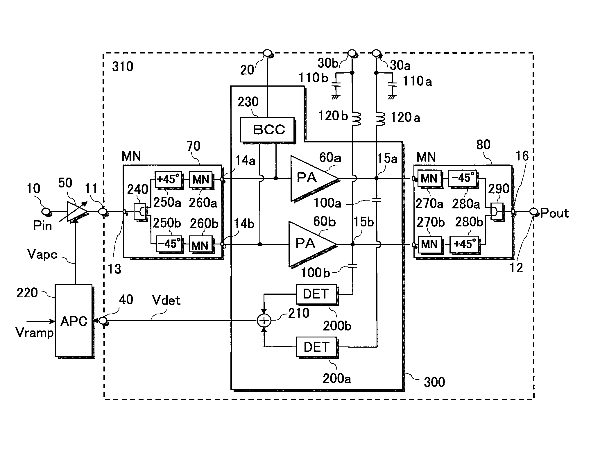
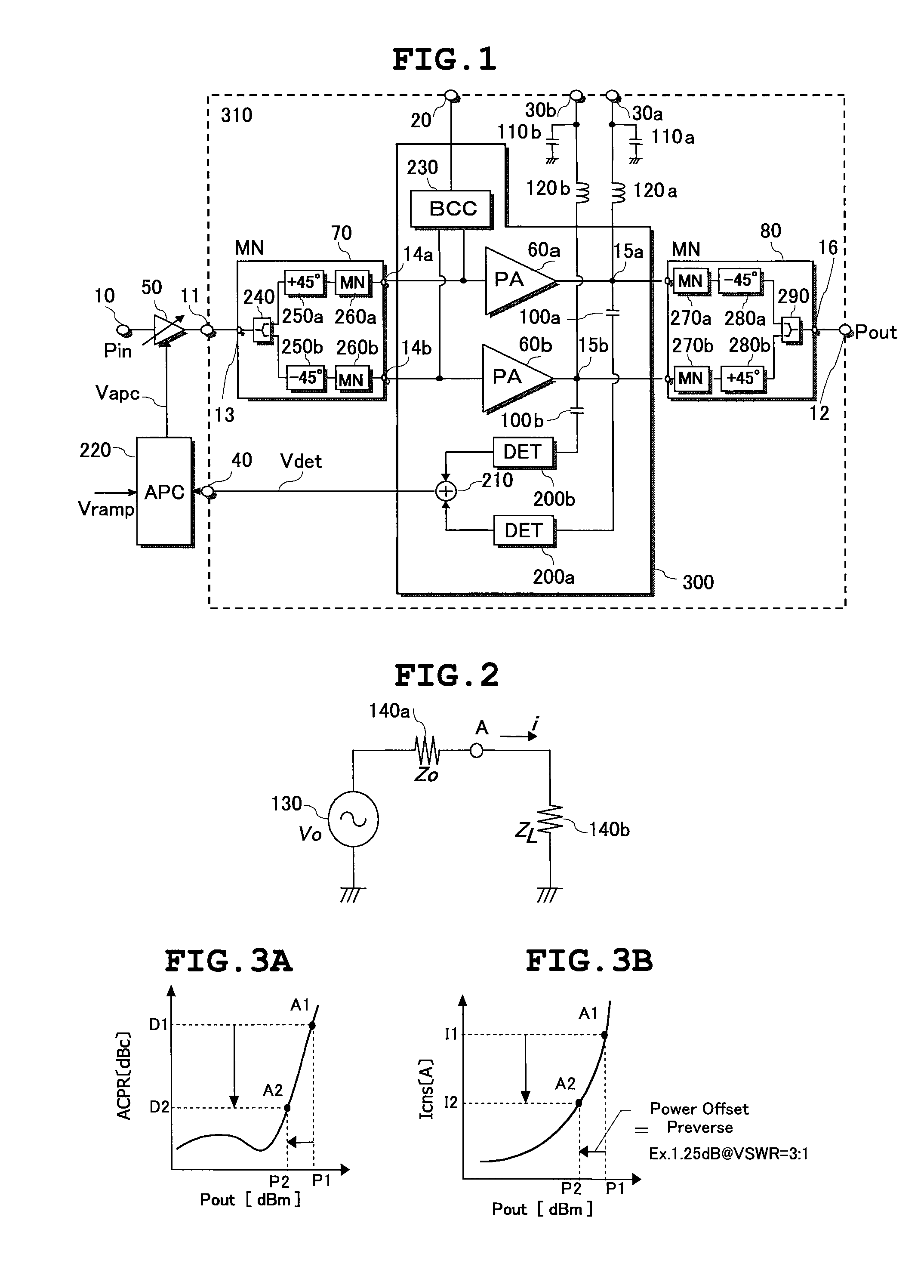
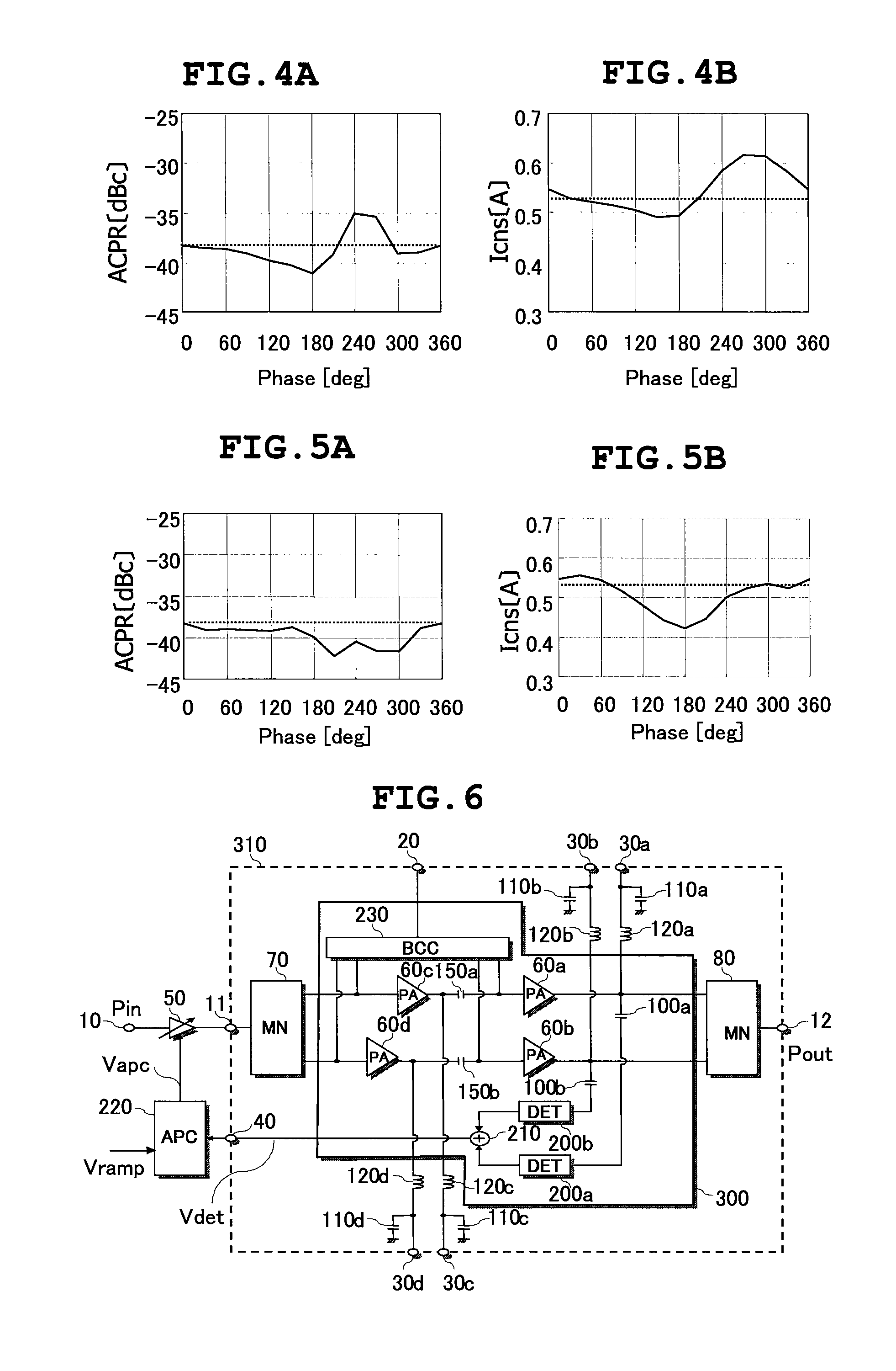
[0036][1] A RF (Radio Frequency) power amplifying device (310) according to a preferred embodiment of the present invention includes a first RF power amplifier (60a) and a second RF power amplifier (60b).

[0037]The RF power amplifying device includes first phase shifters (250a and 250b) arranged on input sides of the first RF power amplifier and the second RF power amplifier and second phase shifters (280a and 280b) arranged on output sides of the first RF power amplifier and the second RF power amplifier.

[0038]The RF power amplifying device is constituted by a system of a balanc...


PUM


Abstract

A RF power amplifying device is constituted by a system of a balanced amplifier including first phase shifters, a first RF power amplifier, a second RF power amplifier, second phase shifters, and a power combiner. Transmitting power Pout is detected by a first power level detector connected to an output of the first RF power amplifier, a second power level detector connected to an output of the second RF power amplifier, and an adder. A level control signal from a level control circuit controls transmitting power in response to a transmitting signal with wanted power level and a detected signal of the adder.

Description

CLAIM OF PRIORITY[0001]The present application claims priority from Japanese application JP 2006-318533 filed on Nov. 27, 2006, the content of which is hereby incorporated by reference into this application.FIELD OF THE INVENTION[0002]The present invention relates to a RF (Radio Frequency) power amplifying device and a wireless communication terminal device and a mobile wireless communication terminal mounted with the RF power amplifying device, and, more particularly to a technique useful for improving performance without using an isolator and a directional coupler.BACKGROUND OF THE INVENTION[0003]There are plural communication systems in mobile communication represented by a cellular phone. For example, in Europe, in addition to GSM widely used as a second generation for wireless communication system and EDGE in which data communication rate of GSM is improved, there is W-CDMA as a third generation for wireless communication system brought into operation in recent years. In North ...

Claims


Application Information

Patent Timeline
Patent Type & Authority Patents(United States)
IPC IPC(8): H04B1/04H04K3/00
CPCH03F1/0205H03F1/0211H03F1/0261H03F3/195H03F3/211H03F3/24H03G3/3047H03F2200/111H03F2200/393H03F2200/405H03F2200/451H03F2200/465H03F2203/21103H03F2203/21112H03F2203/21139H03F2203/21142H03F2203/21157H04B2001/0416
Inventor KURIYAMA, AKIRAMATSUMOTO, HIDETOSHI
Owner RENESAS ELECTRONICS CORP
Why Eureka
Try Eureka