

Pressurized underfill cure
a technology of underfill and cure, which is applied in the direction of electrical equipment, semiconductor devices, semiconductor/solid-state device details, etc., can solve the problems of voids entrapped inside the underfill material, c4 connections are susceptible to mechanical stress, and semiconductor chips fail during use, so as to achieve fast temperature ramping and maintain viscosity
- Summary
- Abstract
- Description
- Claims
- Application Information
AI Technical Summary
Benefits of technology
Problems solved by technology
Method used
Image

Examples
first embodiment
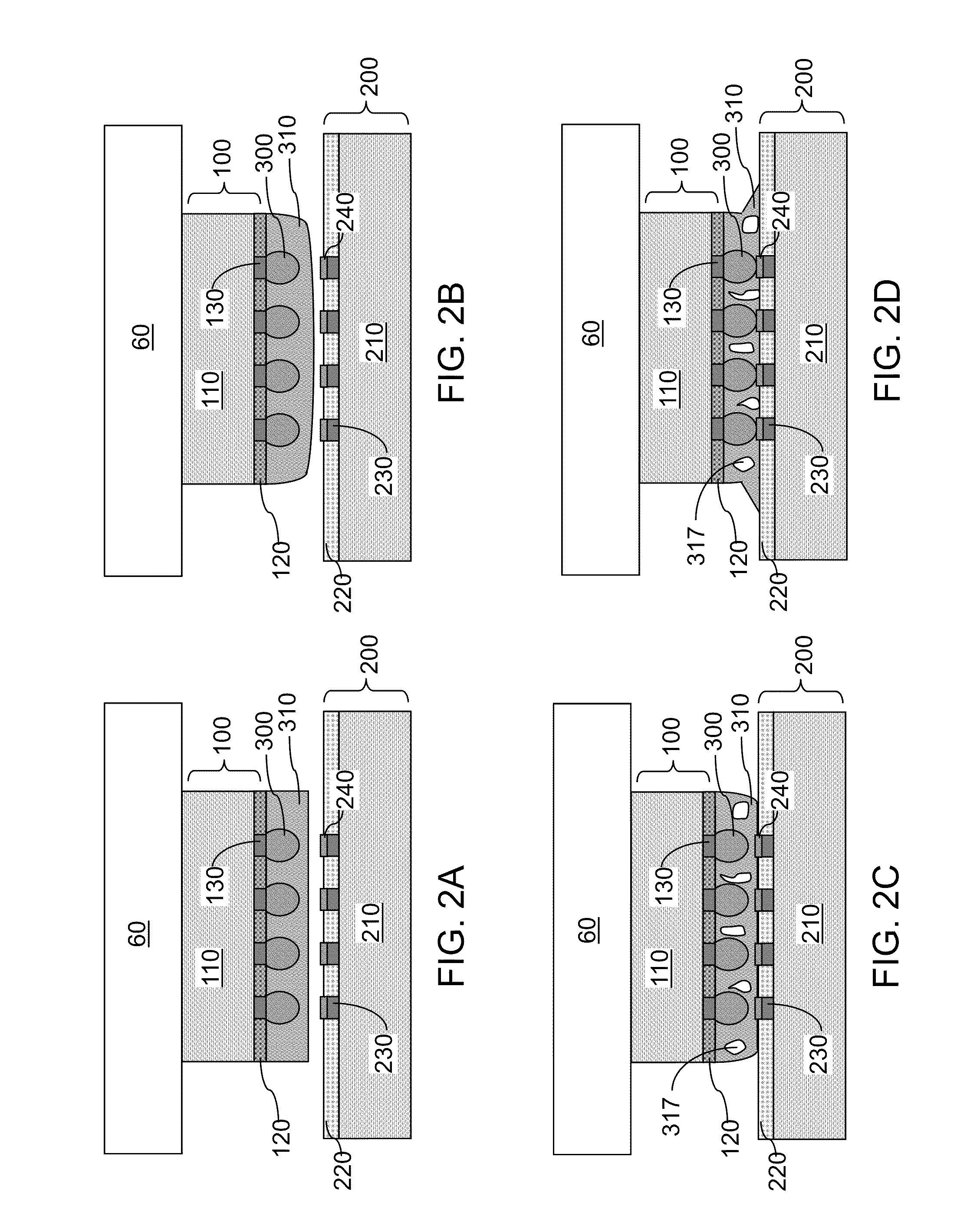
[0060]Referring to FIG. 4A, a set of graphs illustrate conditions for a first cure process according to the present disclosure. At time t0, which is herein referred to as a process starting time, the temperature of an assembly of a first substrate 100 and a second substrate 200, as provided in FIG. 2F or in FIG. 3D, is placed in a pressurization chamber, which can be the enclosure 360 illustrated in FIG. 2G. Once the pressurization chamber is sealed, the assembly of the first substrate 100 and the second substrate 200 with an underfill material 310 and voids 317 is subjected processing conditions.
[0061]The pressure of the processing conditions is shown in a pressure curve 400, and the temperature of the processing conditions is shown in a temperature curve 410. The pressure of the processing conditions can be modified as shown in an alternate pressure curve 402, or any curve between the pressure curve 400 and the alternate pressure curve 402. The temperature of the processing condit...
second embodiment
[0070]Referring to FIG. 5A, a set of graphs illustrate conditions for a second cure process according to the present disclosure. The pressure of the processing conditions is shown in a pressure curve 500, and the temperature of the processing conditions is shown in a temperature curve 510. The temperature of the processing conditions can be modified as shown in an alternate initial temperature curve 511 or any curve between the temperature curve 510 and the alternate initial temperature curve 511. Further, the temperature of the processing conditions can also be modified as shown in an alternate terminal temperature curve 512 or any curve between the temperature curve 510 and the alternate terminal temperature curve 512. The pressure of the processing conditions can be modified as shown in an alternate pressure curve 502 or any curve between the pressure curve 500 and the alternate pressure curve 502.
[0071]In the second cure process, the single cure temperature employed in the first...
third embodiment
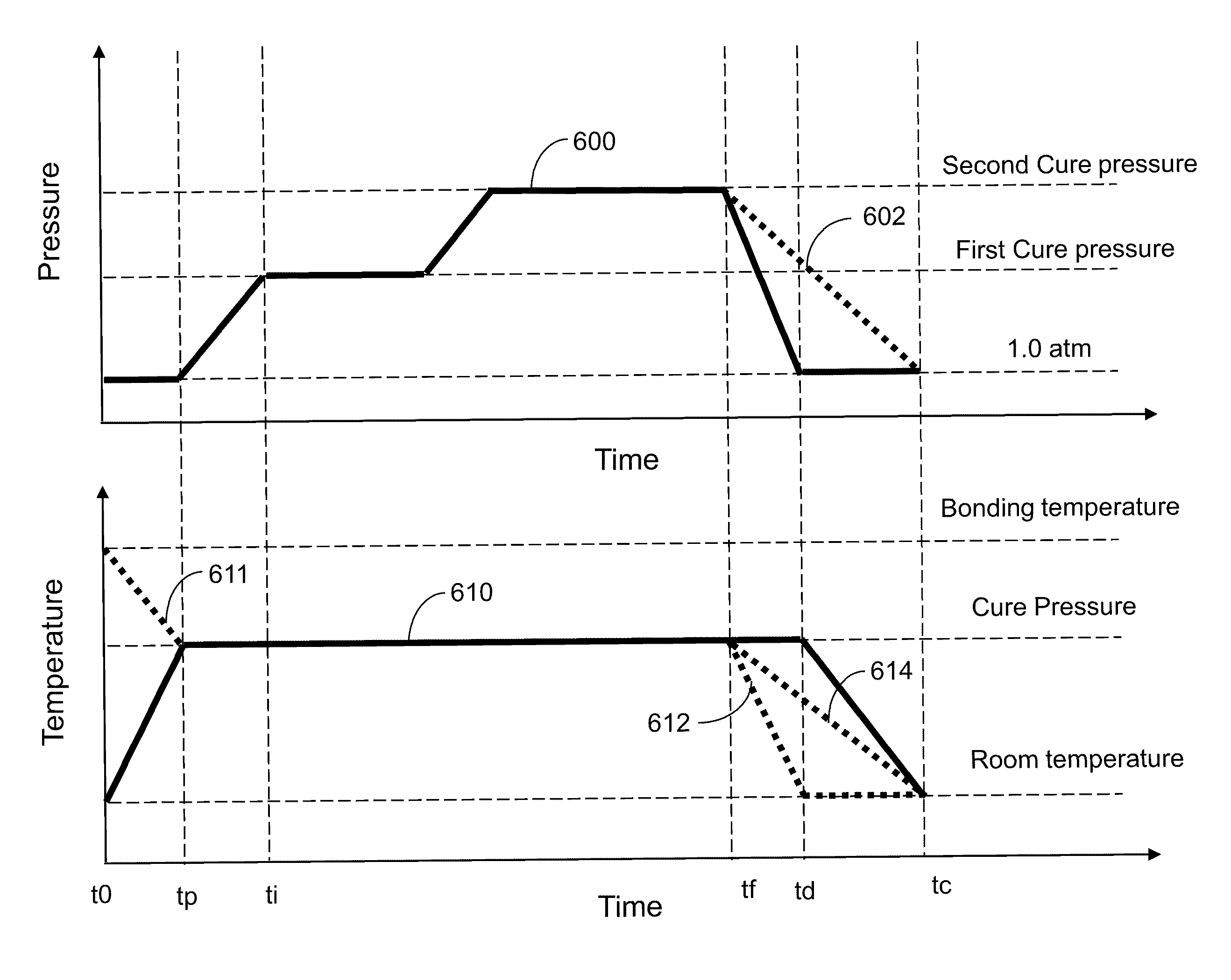
[0076]Referring to FIG. 6A, a set of graphs illustrate conditions for a third cure process according to the present disclosure. The pressure of the processing conditions is shown in a pressure curve 600, and the temperature of the processing conditions is shown in a temperature curve 610. The temperature of the processing conditions can be modified as shown in an alternate initial temperature curve 611 or any curve between the temperature curve 610 and the alternate initial temperature curve 611. Further, the temperature of the processing conditions can also be modified as shown in an alternate terminal temperature curve 612 or any curve between the temperature curve 610 and the alternate terminal temperature curve 612. The pressure of the processing conditions can be modified as shown in an alternate pressure curve 602 or any curve between the pressure curve 600 and the alternate pressure curve 602.
[0077]In the third cure process, the single cure pressure employed in the first cure...
PUM
 Abstract
Description
Claims
Application Information