Ion gate for dual ion mobility spectrometer and method thereof
a technology of mobility spectrometer and ion gate, which is applied in the field of ion gate, can solve the problems of low effective high production cost, and strict assembly requirements, and achieve the effect of improving the utility rate of ions
- Summary
- Abstract
- Description
- Claims
- Application Information
AI Technical Summary
Benefits of technology
Problems solved by technology
Method used
Image
Examples
first embodiment
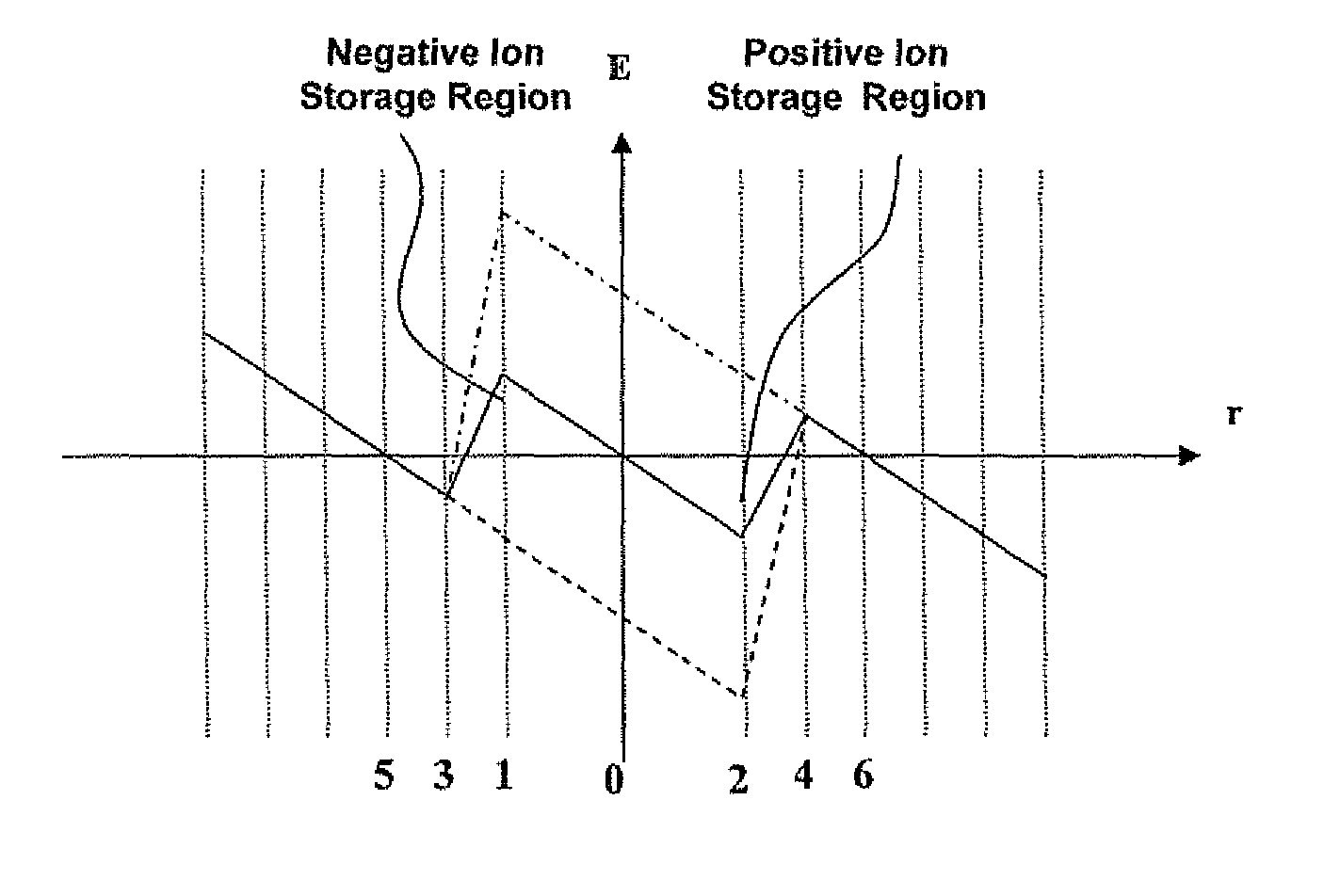
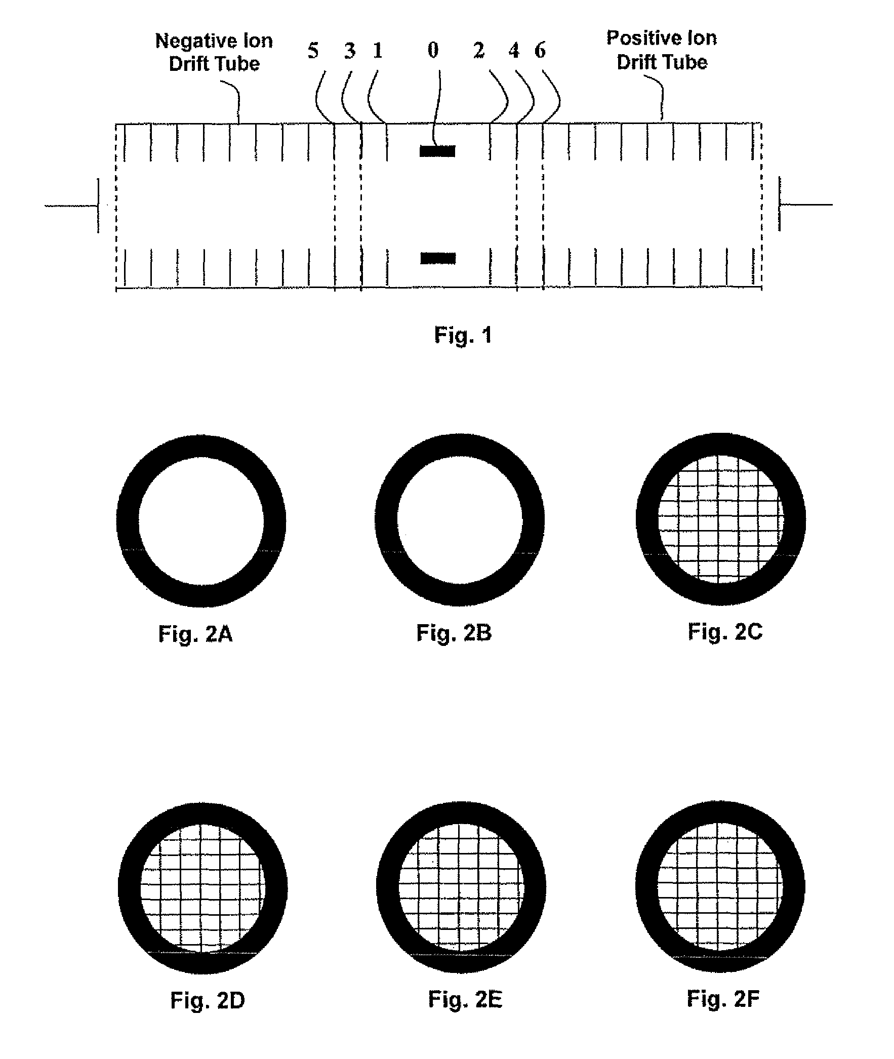
[0030]FIG. 1 shows an ion gate for positive and negative ions used in a dual IMS. The ion gate is provided with an ion source 0, a first gate electrode 1, a second gate electrode 2, a third gate electrode 3 and a fourth gate electrode 4. The second gate electrode 2 is located between the ion source 0 and the fourth gate electrode 4, and the first gate electrode 1 is located between the ion source 0 and the third gate electrode 3. Further, a fifth gate electrode 5 can be the initial part of a drift tube for detecting negative ions, and a sixth gate electrode 6 can be the initial part of a drift tube for detecting positive ions. With respect to the ion source 0, the first, third and fifth gate electrodes 1, 3, 5 are arranged in symmetry with the second, fourth and sixth gate electrodes 2, 4, 6.
[0031]The ion source 0 serves to ionize sample molecules. The ion source can be a radioactive isotope, laser and the like. Each of the first and second gate electrodes 1, 2 is a plate having a h...
second embodiment
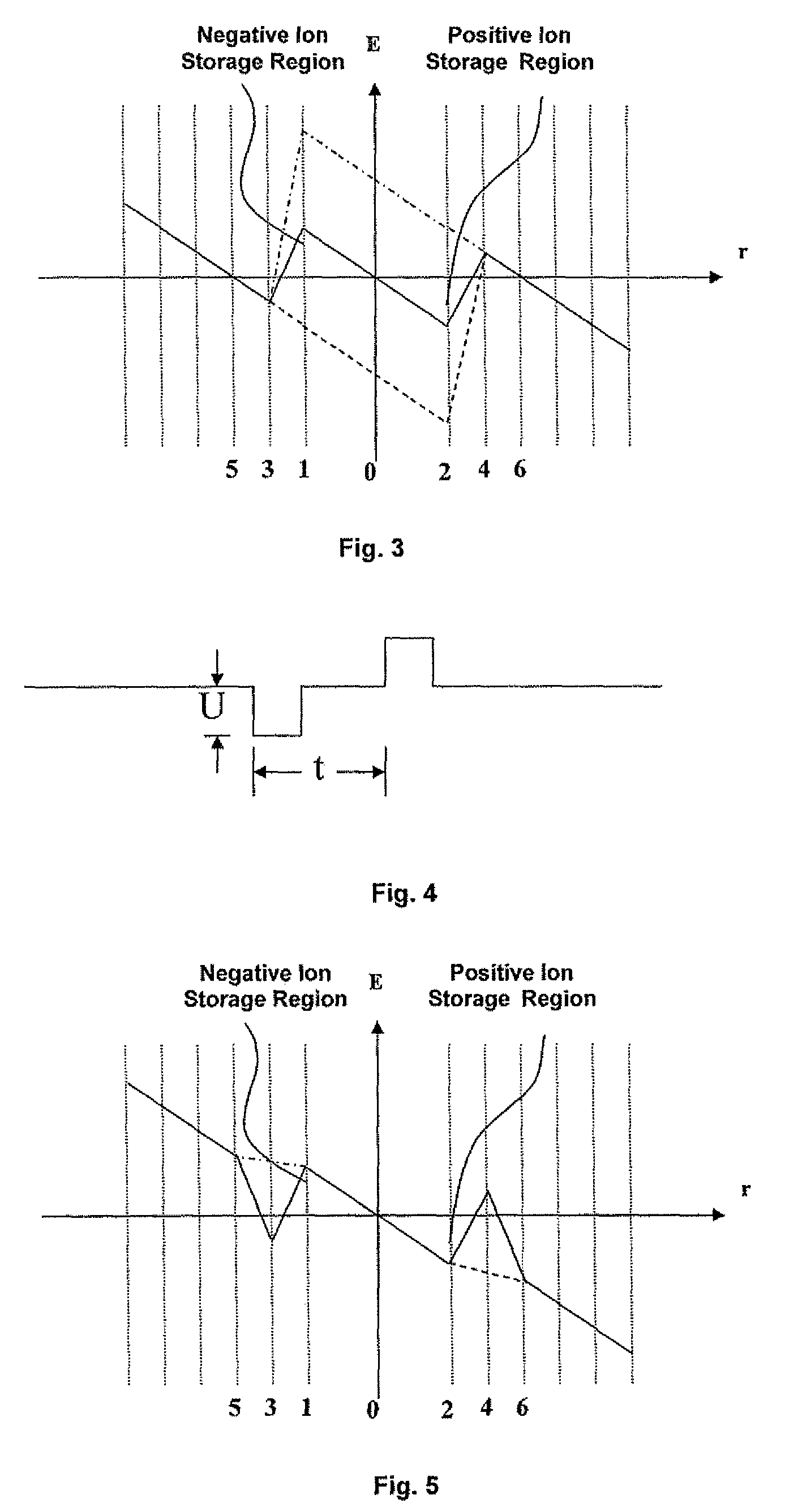
[0042]FIG. 5 is a schematic graph of the distribution of potentials along the tube axis during the ion storage and eduction according to the second embodiment of the present invention.
[0043]As shown in FIG. 5, according to the second embodiment of the present invention, the respective electrodes and the ion source are applied with voltages during the ion storage phase so that the potentials along the tube axis of the ion gate fulfill the relationship: the potential at the fifth gate electrode 5>the potential at the first gate electrode 1>the potential at the ion source 0>the potential at the third gate electrode 3, and accordingly a negative ion storage region for storing negative ions is formed adjacent to the first gate electrode 1; and the potential at the sixth gate electrode 6204, and accordingly a positive ion storage region for storing positive ions is formed adjacent to the second gate electrode 2.
[0044]During the phase of eduction of negative ion, a negative pulse is applie...
third embodiment
[0055]FIG. 6 is a schematic graph of the distribution of potentials along the tube axis during the ion storage and eduction according to the third embodiment of the present invention.
[0056]the respective electrodes and the ion source are applied with voltages during the ion storage phase so that the potentials along the tube axis of the ion gate fulfill the relationship: the potential at the first gate electrode 1>the potential at the fifth gate electrode 5=the potential at the ion source 0>the potential at the third gate electrode 3, and accordingly a negative ion storage region is formed adjacent to the first gate electrode 1; and the potential at the second gate electrode 20=the potential at the sixth gate electrode 64, and accordingly a positive ion storage region is formed adjacent to the second gate electrode 2.
[0057]During the phase of negative ion eduction, the negative ions are educed by controlling only the potential at the ion source 0, requiring a negative pulse having a...
PUM
| Property | Measurement | Unit |
|---|---|---|
| ion transmittance | aaaaa | aaaaa |
| time | aaaaa | aaaaa |
| inner radius | aaaaa | aaaaa |
Abstract
Description
Claims
Application Information


