Betavoltaic battery with a shallow junction and a method for making same

a technology of betavoltaic batteries and shallow junctions, applied in the field of betavoltaic batteries with shallow junctions and a method for making same, can solve the problem of not being able to provide power generation, and achieve the effect of reducing or eliminating losses through electron-hole pair recombination

Active Publication Date: 2011-09-13
WIDETRONIX
View PDF7 Cites 19 Cited by
  • Summary
  • Abstract
  • Description
  • Claims
  • Application Information

AI Technical Summary

Benefits of technology

[0010]Thus, with knowledge of a lower energy beta-electron's path length, it is desirable to create thin, or ultra-shallow, junctions, which enable even the lowest energy electrons to penetrate well into the depletion region. This invention is a betavoltaic device comprising ultra-shallow junctions which allow such penetration of emitted lower energy electrons, thus, reducing or eliminating losses through electron-hole pair recombination at the surface (see FIG. 1).

Problems solved by technology

If electron-hole pairs created by low energy beta-electrons are generated near the surface of a device, they will recombine there, due to interaction with surface states (i.e. defects occurring at the termination site of crystals and serving as sites for minority carrier loss), and will not be available for power generation.

Method used


Image

  • Betavoltaic battery with a shallow junction and a method for making same
  • Betavoltaic battery with a shallow junction and a method for making same
  • Betavoltaic battery with a shallow junction and a method for making same

Examples


Embodiment Construction

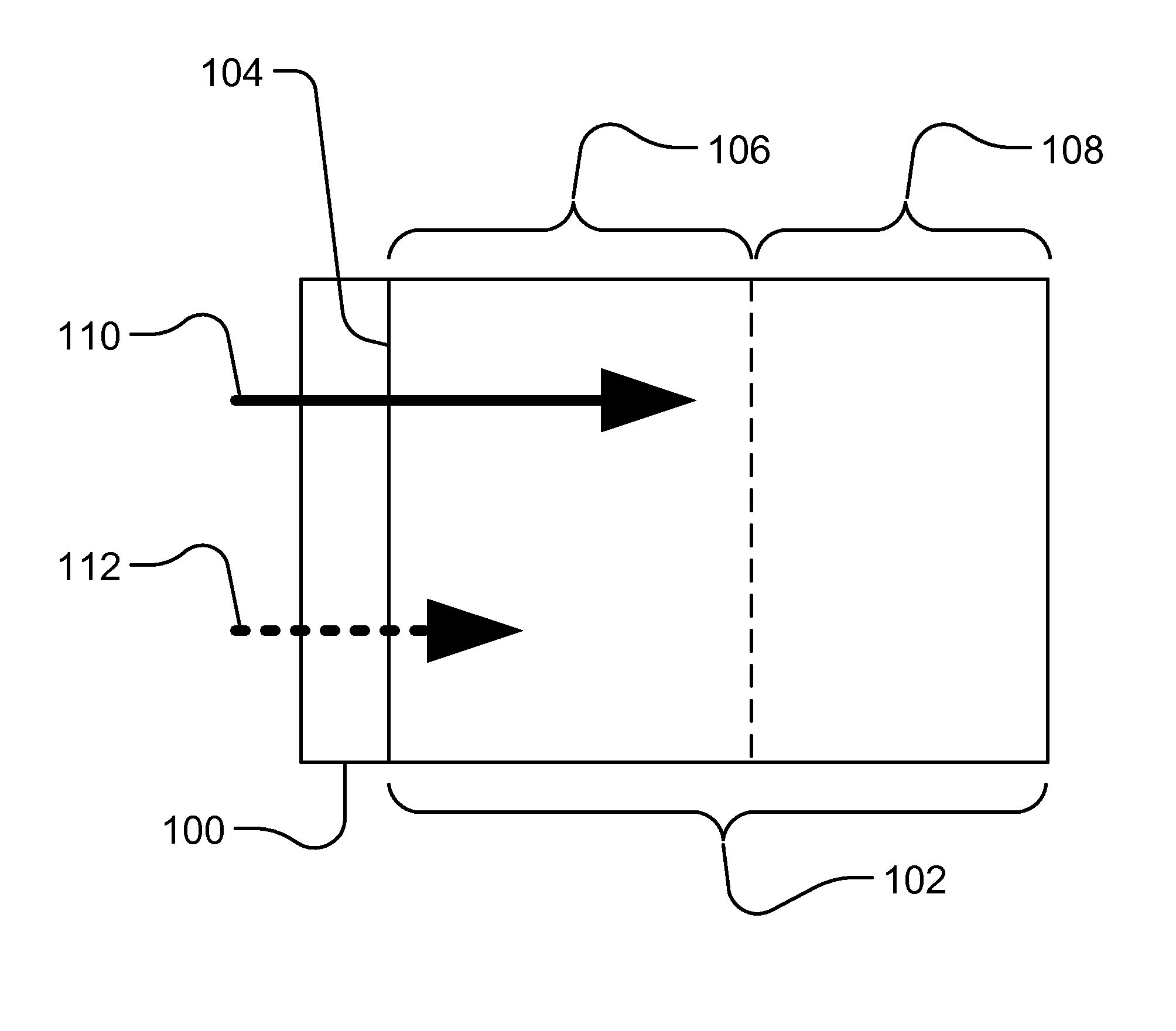
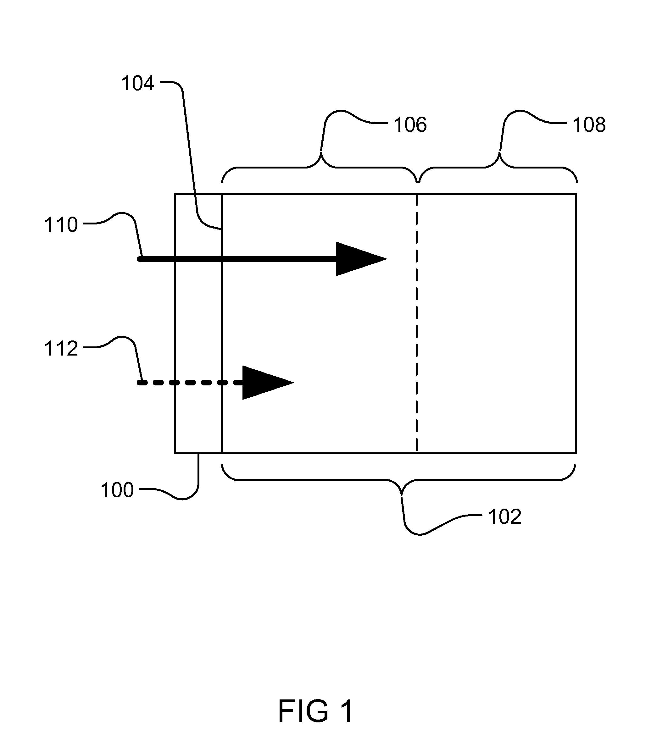
Maximizing Charge Collection in SiC Betavoltaics

Influence of Junction Depth

[0016]To quantify the extent of the surface, it is necessary to know the penetration depth, or range, RB in μm, of the beta electron in the semiconductor, which is given as:

RB(μm)=[4×E01.75(keV) / 100] / ρ(g / cm3)  (1),

where E0 is the incident beta energy in keV, and ρ is the density of the semiconductor in g / cm3. The penetration depth is simply a function of the energy spectrum of the β-radiation, which is known. The spectrum, to first order, is given by

ƒ(E0)=K√{square root over (E02+2mc2E0)}(E0(max)−E0)2  (2)

where f(E) is the energy distribution function, m the electronic mass, c the speed of light, and K a normalization constant, such that we have:

[0017]∫0E0(max)⁢f⁡(E0)⁢⁢ⅆE0=1(3)

[0018]The energy extends to a maximum, E0(max), that typically lies at ˜3 times the mean energy. For a given beta emitting isotope, a single E0(max) completely specifies the spectrum, as eq. 2 indicates. There is a Coulombic penetration...


PUM


Abstract

This is a novel SiC betavoltaic device (as an example) which comprises one or more “ultra shallow” P+N− SiC junctions and a pillared or planar device surface (as an example). Junctions are deemed “ultra shallow”, since the thin junction layer (which is proximal to the device's radioactive source) is only 300 nm to 5 nm thick (as an example). In one example, tritium is used as a fuel source. In other embodiments, radioisotopes (such as Nickel-63, promethium or phosphorus-33) may be used. Low energy beta sources, such as tritium, emit low energy beta-electrons that penetrate very shallow distances (as shallow as 5 nm) in semiconductors, including SiC, and can result in electron-hole pair creation near the surface of a semiconductor device rather than pair creation in a device's depletion region. By contrast, as a high energy electron penetrates a semiconductor device surface, such as a diode surface, it produces electron hole-pairs that can be collected at (by drift) and near (by diffusion) the depletion region of the device. This is a betavoltaic device, made of ultra-shallow junctions, which allows such penetration of emitted lower energy electrons, thus, reducing or eliminating losses through electron-hole pair recombination at the surface.

Description

RELATED APPLICATIONS[0001]This current application is a continuation of (related to) a prior provisional application, Ser. No. 61 / 250,504, filed 10 Oct. 2009, with the same inventor(s), same assignee (Widetronix Corporation), and the same title.BACKGROUND OF THE INVENTION[0002]There are several technical constraints that must be considered when designing a low cost, manufacturable, high volume, high power density silicon carbide (SiC) betavoltaic device. First, consideration must be given to the energy profile of radioisotopes to be used, and the volume at which such material can be produced. For example, tritium is one of the several viable radioisotope candidates, since it can be produced in sufficient quantities to support high volume device manufacture, and its energy profile fits well with a range of power generation design parameters.[0003]Secondly, in order to produce high power density in betavoltaics, a large device surface area is required. There are issued and pending bet...

Claims


Application Information

Patent Timeline
Patent Type & Authority Patents(United States)
IPC IPC(8): H01L21/00
CPCG21H1/02G21H1/06H01L21/02625H01L21/02529H01L21/02579H01L21/02378
Inventor SPENCER, MICHAELCHANDRASHEKHAR, MVS
Owner WIDETRONIX
Why Eureka
Try Eureka