Organic light-emitting element, image display device and production method thereof

a technology of light-emitting elements and image display devices, which is applied in the direction of discharge tube luminescnet screens, natural mineral layered products, transportation and packaging, etc., can solve the problems of element reliability, degradation of light-emitting layers, and element reliability

Active Publication Date: 2011-09-27
SAMSUNG DISPLAY CO LTD +1
View PDF14 Cites 27 Cited by
  • Summary
  • Abstract
  • Description
  • Claims
  • Application Information

AI Technical Summary

Benefits of technology

[0009]It is an object of the present invention to provide an organic element emitting white light of high structural reliability. It is another object to apply the same element to display devices. It is still another object to apply the same element to illuminators for liquid-crystal display devices. It is still another object to provide a structure capable of reducing light interference effects, which may occur as laminated film thickness increases.
[0025]The anode for the present invention is preferably of an electroconductive film of high work function, which can enhance hole injection efficiency. More specifically, the materials useful for the present invention include, but not limited to, gold and platinum.
[0047]Thickness of the mixed light-emitting layer can be within a range from 1 to 100 nm. It should be noted, however, that the carrier is trapped by the dopant in the mixed light-emitting layer, and increasing layer thickness decreases carrier transport capacity of the layer. Therefore, its thickness is preferably in a range from 1 to 10 nm.
[0076]The mixed light-emitting layer for the present invention traps carriers by the dopant contained therein. Consequently, increasing a dopant content of the light-emitting layer, which comprises a transport material of high mobility, enhances a charge balance in the layer and hence its light-emitting efficiency.
[0083]The protective layer is provided on the second electrode, to prevent H2O and O2 in air from entering the second electrode or organic layer below the second electrode.
[0096]In an active matrix type device, on the other hand, 2 to 4 driving elements, each composed of a switching element of thin-film transistor and capacitor, are connected to the organic EL (light-emitting) element which constitutes a pixel. As a result, all pixels can be on in a frame period to extend service life of the organic light-emitting element, because necessity for increasing brightness is removed.

Problems solved by technology

This may cause degradation of the light-emitting layer through which carriers move and hence problems related to element reliability.
In the element disclosed by Patent Document 2, on the other hand, carriers of low transport capacity should move through a transport layer of high transport capacity material, which may also cause problems related to element reliability.

Method used


Image

  • Organic light-emitting element, image display device and production method thereof
  • Organic light-emitting element, image display device and production method thereof
  • Organic light-emitting element, image display device and production method thereof

Examples


example 1

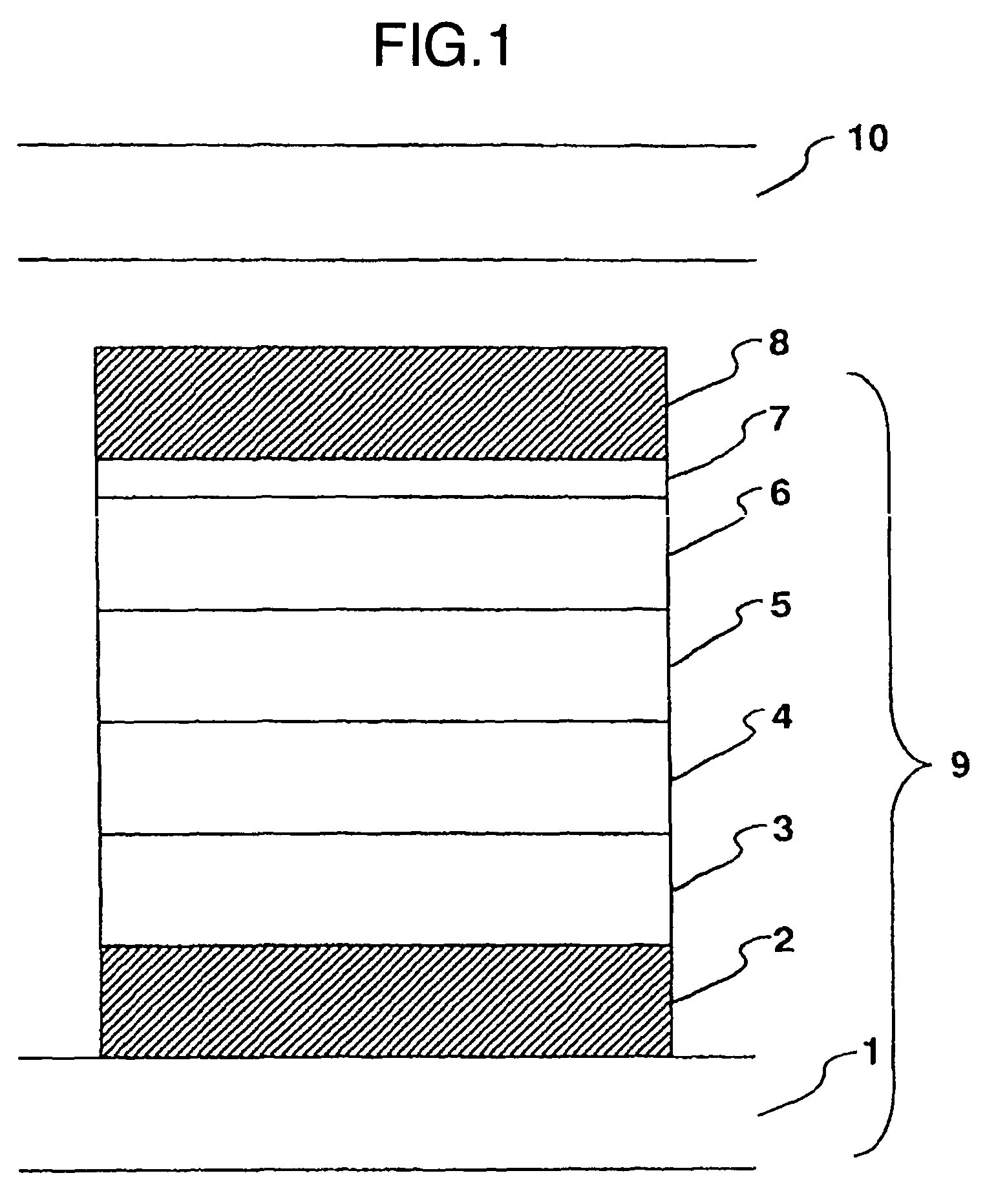
[0204]First, one embodiment of the laminated layer comprising 2 mixed light-emitting layers is described by referring to FIG. 1, wherein 1: glass board, 2: lower electrode, 3: hole transport layer, 4: first mixed light-emitting layer, 5: second mixed light-emitting layer, 6: electron transport layer, 7: electron injection layer, 8: upper electrode, 9: organic EL board, and 10: sealing board.

[0205]A 150 nm thick ITO film was formed on the glass board 1 by sputtering, and was treated by photolithography to form the lower electrode 2.

[0206]Next, the lower electrode 2 was coated with a 50 nm thick film of 4,4-bis[N-(1-naphthyl)-N-phenylamino]biphenyl (hereinafter referred to as α-NPD) by vacuum deposition.

[0207]A starting material for α-NPD, put in a sublimation boat of molybdenum, was deposited on the lower electrode 2, where the deposition rate was controlled at 0.15±0.01 nm / second. The α-NPD film worked as the hole transport layer 3.

[0208]Next, the hole transport layer 3 was coated w...

example 2

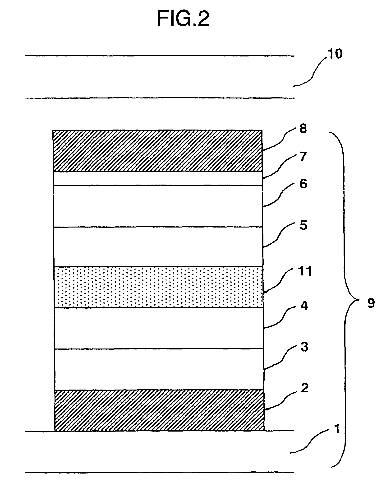
[0229]Next, another embodiment of the laminated layer with a mixed transport layer placed between 2 mixed light-emitting layers is described by referring to FIG. 2, wherein 11: mixed transport layer.

[0230]A 150 nm thick Cr film was formed on the glass board 1 by sputtering, and was treated by photolithography to form the lower electrode 2.

[0231]The lower electrode 2 was coated with the hole transport layer 3 and first mixed light-emitting layer 4 in the same manner as in EXAMPLE 1.

[0232]Next, the first mixed light-emitting layer 4 was coated with a 15 nm thick codeposited film of HMTPD and BCP by vacuum deposition on. Starting materials for HMTPD and BCP, each put in a sublimation boat of molybdenum, were codeposited, where the deposition rate was controlled at 0.20±0.01 nm / second for these materials. The codeposited film worked as the mixed transport layer 11.

[0233]Next, the mixed transport layer 11 was coated with the second mixed light-emitting layer 5 in the same manner as in EX...

example 3

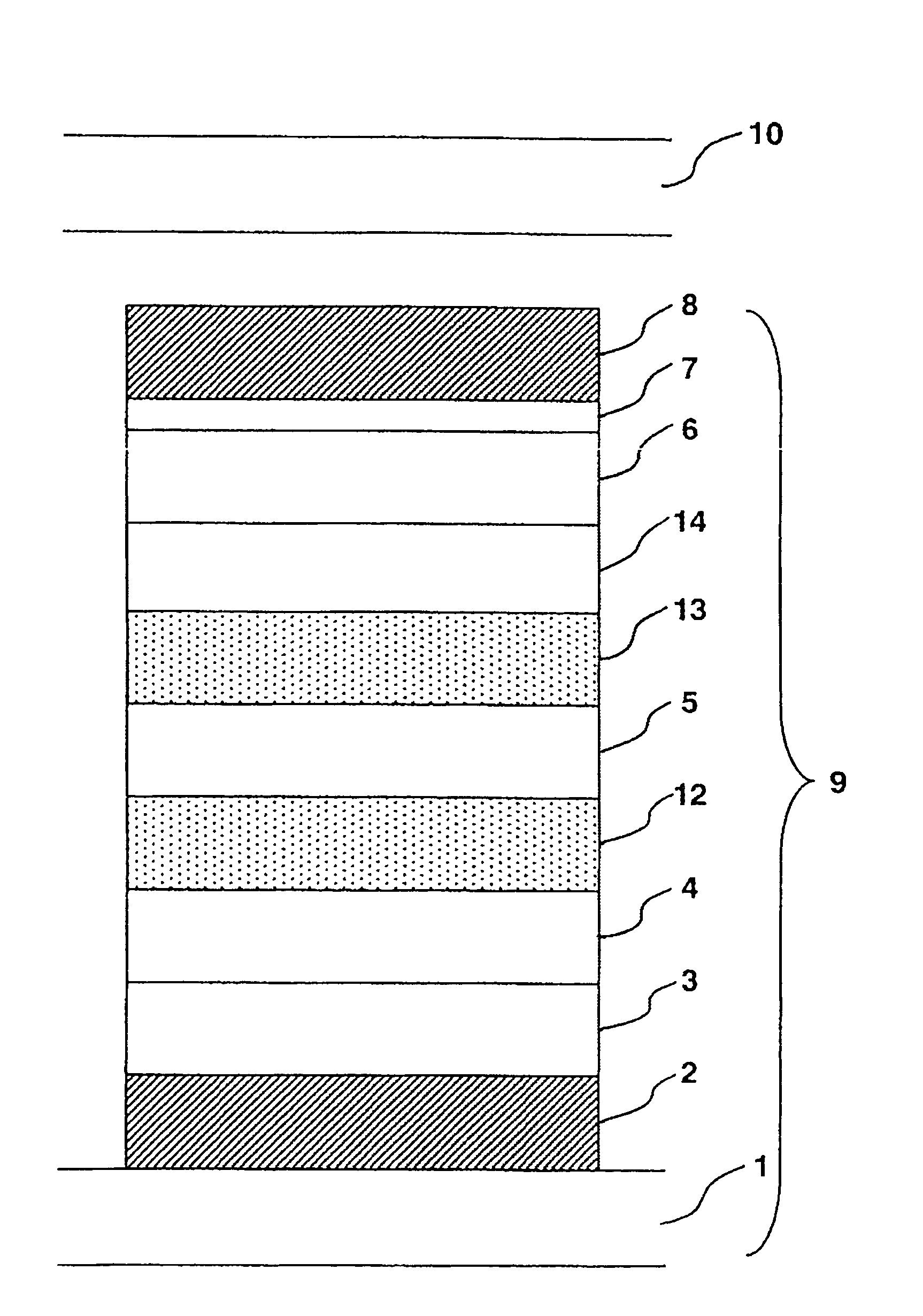
[0254]Next, still another embodiment of the laminated layer having 3 mixed light-emitting layers with 2 mixed transport layers each placed between the mixed light-emitting layers is described by referring to FIG. 3, wherein 12: first mixed transport layer, 13: second mixed light-emitting layer and 14: third mixed light-emitting layer.

[0255]The glass board 1 was coated with the lower electrode 2, hole transport layer 3 and the first mixed light-emitting layer 4 in the same manner as in EXAMPLE 1.

[0256]Next, the first mixed light-emitting layer 4 was coated with a 15 nm thick codeposited film of HMTPD and BCP by vacuum deposition. Starting materials for HMTPD and BCP, each put in a sublimation boat of molybdenum, were codeposited, where the deposition rate was controlled at 0.20±0.01 nm / second for these materials. The codeposited film worked as the first mixed transport layer 12.

[0257]Next, the first mixed transport layer 12 was coated with a 5 nm thick codeposited film of α-NPD, Alq3...


PUM

PropertyMeasurementUnit
thicknessaaaaaaaaaa
thicknessaaaaaaaaaa
work functionaaaaaaaaaa

Abstract

It is an object to provide an organic light-emitting element having two or more light-emitting layers, wherein degradation of each constituent material for the light-emitting layer is reduced to improve reliability of the element. The present invention provides an organic light-emitting element having a laminated structure with a first mixed light-emitting layer 4 composed of a hole transport material, an electron transport material and a dopant which determines a color of an emitted light, and a second mixed light-emitting layer 5 composed of a hole transport material, an electron transport material and a dopant which determines a color of an emitted light, and also provides an image display device which uses the organic light-emitting element.

Description

FIELD OF THE INVENTION[0001]The present invention relates to an organic light-emitting element of self-luminosity, image display device using the same element, and production method thereof.BACKGROUND OF THE INVENTION[0002]An organic electroluminescent element emitting white light (hereinafter referred to as organic element emitting white light) has been expected to go into various devices, e.g., thin display devices, illuminator for display devices and illuminator.[0003]Patent Document 1 discloses a structure of organic element emitting white light. It has two light-emitting layers, one emitting a blue color on the anode side and the other a yellow to red color on the cathode side, where each layer contains a dopant which determines color of emitted light. It discloses a 10 nm thick layer for emitting a blue color and 40 nm thick layer for emitting a yellow to red color in EXAMPLE 1, suggesting a low hole transport capacity of the material for the blue-emitting layer.[0004]A materi...

Claims


Application Information

Patent Timeline
Patent Type & Authority Patents(United States)
IPC IPC(8): H01L51/50C09K11/06H01L51/52H05B33/12H05B33/14H05B33/22
CPCH01L51/5036H01L51/5008H05B33/14H01L51/5048H01L51/5096H01L51/5271Y10T428/24942Y10S428/917Y10T428/26H10K30/865H10K50/125H10K50/14H10K50/18H10K50/856
Inventor ISHIHARA, SHINGOARATANI, SUKEKAZUADACHI, MASAYAOUCHI, TAKAYUKI
Owner SAMSUNG DISPLAY CO LTD
Why Eureka
Try Eureka