Epitaxial growth of in-plane nanowires and nanowire devices

a nanowire and in-plane technology, applied in the field of nanowires, can solve the problems of reducing the density and practicality of nanowire devices and circuits, and achieve the effect of minimizing exposure to laboratory air and associated contaminants

Active Publication Date: 2011-10-04
STC UNM
View PDF3 Cites 44 Cited by
  • Summary
  • Abstract
  • Description
  • Claims
  • Application Information

AI Technical Summary

Benefits of technology

[0006]According to various embodiments, the present teachings include a method for forming a nanowire. The nanowire can be formed by first providing a crystalline growth platform. A protection layer can then be formed or disposed on the crystal growth platform, followed by forming a selective growth mask on the protection layer. One or more nanoscale slit-shaped openings can be defined in the selective growth mask with a length oriented along a crystal direction of the crystalline growth platform. A portion of the protection layer in vicinity of each nanoscale slit-shaped opening can be locally removed

Problems solved by technology

Problems arise when growth not vertical to the substrate is desired.
This is a difficult, low yield proce

Method used


Image

  • Epitaxial growth of in-plane nanowires and nanowire devices
  • Epitaxial growth of in-plane nanowires and nanowire devices
  • Epitaxial growth of in-plane nanowires and nanowire devices

Examples


Embodiment Construction

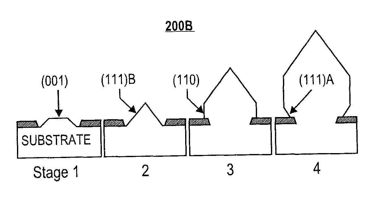
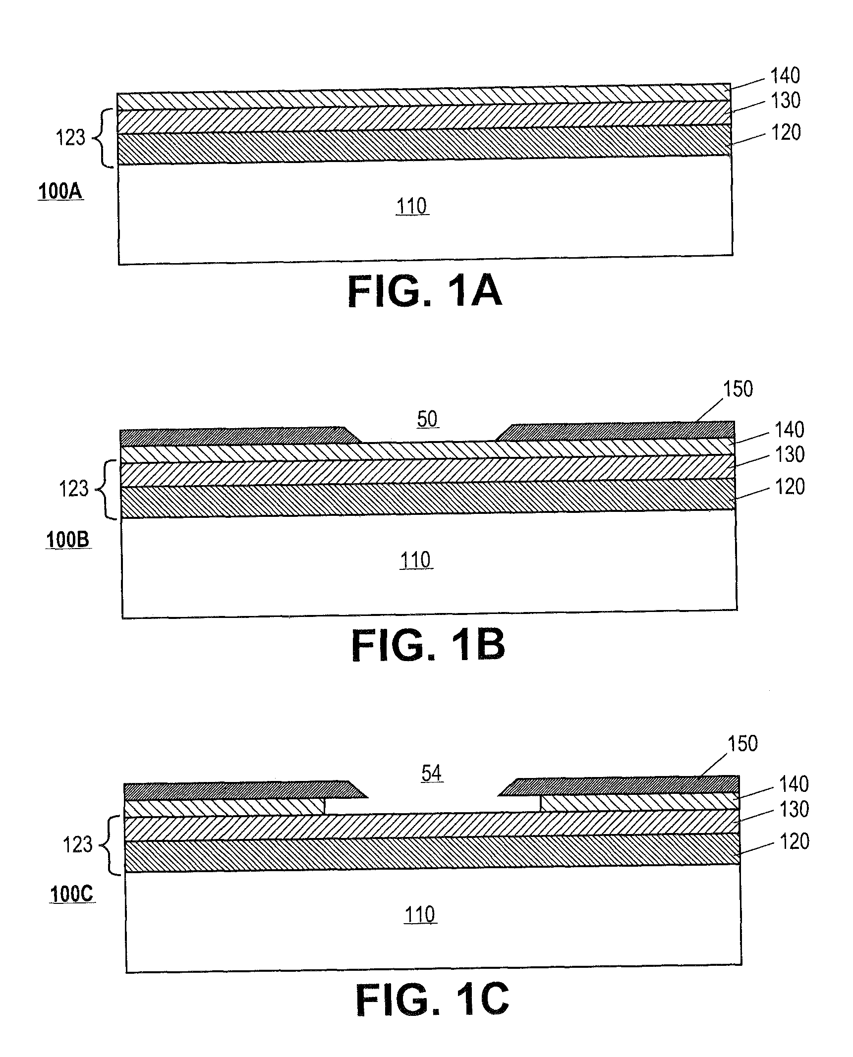
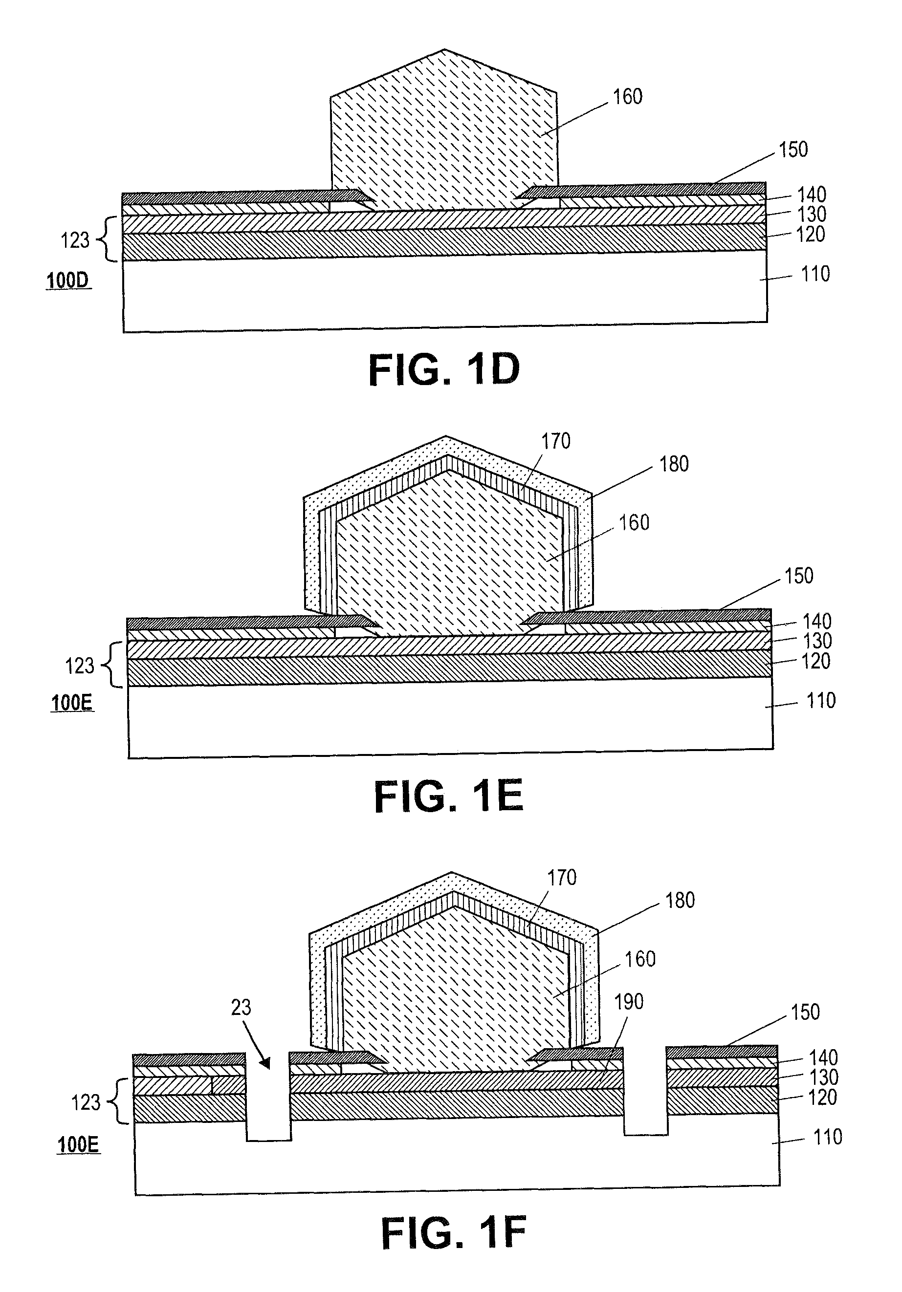
[0023]Reference will now be made in detail to exemplary embodiments of the invention, examples of which are illustrated in the accompanying drawings. Wherever possible, the same reference numbers will be used throughout the drawings to refer to the same or like parts. In the following description, reference is made to the accompanying drawings that form a part thereof, and in which is shown by way of illustration specific exemplary embodiments in which the invention may be practiced. These embodiments are described in sufficient detail to enable those skilled in the art to practice the invention and it is to be understood that other embodiments may be utilized and that changes may be made without departing from the scope of the invention. The following description is, therefore, merely exemplary.

[0024]Exemplary embodiments provide semiconductor nanowires and nanowire devices / applications and methods for making nanowires and related devices. According to various embodiments, in-plane...


PUM


Abstract

Exemplary embodiments provide semiconductor nanowires and nanowire devices/applications and methods for their formation. In embodiments, in-plane nanowires can be epitaxially grown on a patterned substrate, which are more favorable than vertical ones for device processing and three-dimensional (3D) integrated circuits. In embodiments, the in-plane nanowire can be formed by selective epitaxy utilizing lateral overgrowth and faceting of an epilayer initially grown in a one-dimensional (1D) nanoscale opening. In embodiments, optical, electrical, and thermal connections can be established and controlled between the nanowire, the substrate, and additional electrical or optical components for better device and system performance.

Description

RELATED APPLICATIONS[0001]This application claims priority from U.S. Provisional Patent Application Ser. No. 61 / 076,803, filed Jun. 30, 2008, which is hereby incorporated by reference in its entirety.GOVERNMENT RIGHTS[0002]This invention was made with Government support under Contract No. 50615 awarded by the Sandia National Laboratories. The U.S. Government has certain rights in this invention.FIELD OF THE INVENTION[0003]This invention relates generally to nanowires and, more particularly, to in-plane nanowires, in-plane nanowire devices, and methods for their formation.BACKGROUND OF THE INVENTION[0004]Along with the physical dimension, the geometric shape significantly affects the electronic states of semiconductor nanostructures such as quantum dots or nanowires. Most nanowires are epitaxially grown on a patterned substrate and are oriented vertical to the substrate surface. For example, the growth of GaAs from an array of circular apertures patterned on a Si(111) substrate, the ...

Claims


Application Information

Patent Timeline
IPC IPC(8): H01L21/00
CPCB82Y10/00H01L21/0237H01L21/02439H01L21/02521H01L21/02603H01L21/02639H01L29/0665H01L29/0673H01L29/127H01L29/7783H01L21/02507H01L29/158H01S5/32B82Y40/00Y10S977/962H01L29/7853H01L33/06H01L33/18B82Y99/00Y10S977/951
Inventor LEE, SEUNG CHANGBRUECK, STEVEN R. J.
Owner STC UNM
Why Eureka
Try Eureka