Semiconductor structure

a technology of semiconductors and structures, applied in the field of semiconductor structures, can solve the problem that the colloidal oxide can be easily attacked during wet processing

Inactive Publication Date: 2011-10-04
INT BUSINESS MASCH CORP
View PDF7 Cites 13 Cited by
  • Summary
  • Abstract
  • Description
  • Claims
  • Application Information

AI Technical Summary

Problems solved by technology

However, the collar oxide can be attacked easily during wet processing, especially during node dielectric material removal before strap deposition.

Method used


Image

  • Semiconductor structure
  • Semiconductor structure
  • Semiconductor structure

Examples


Embodiment Construction

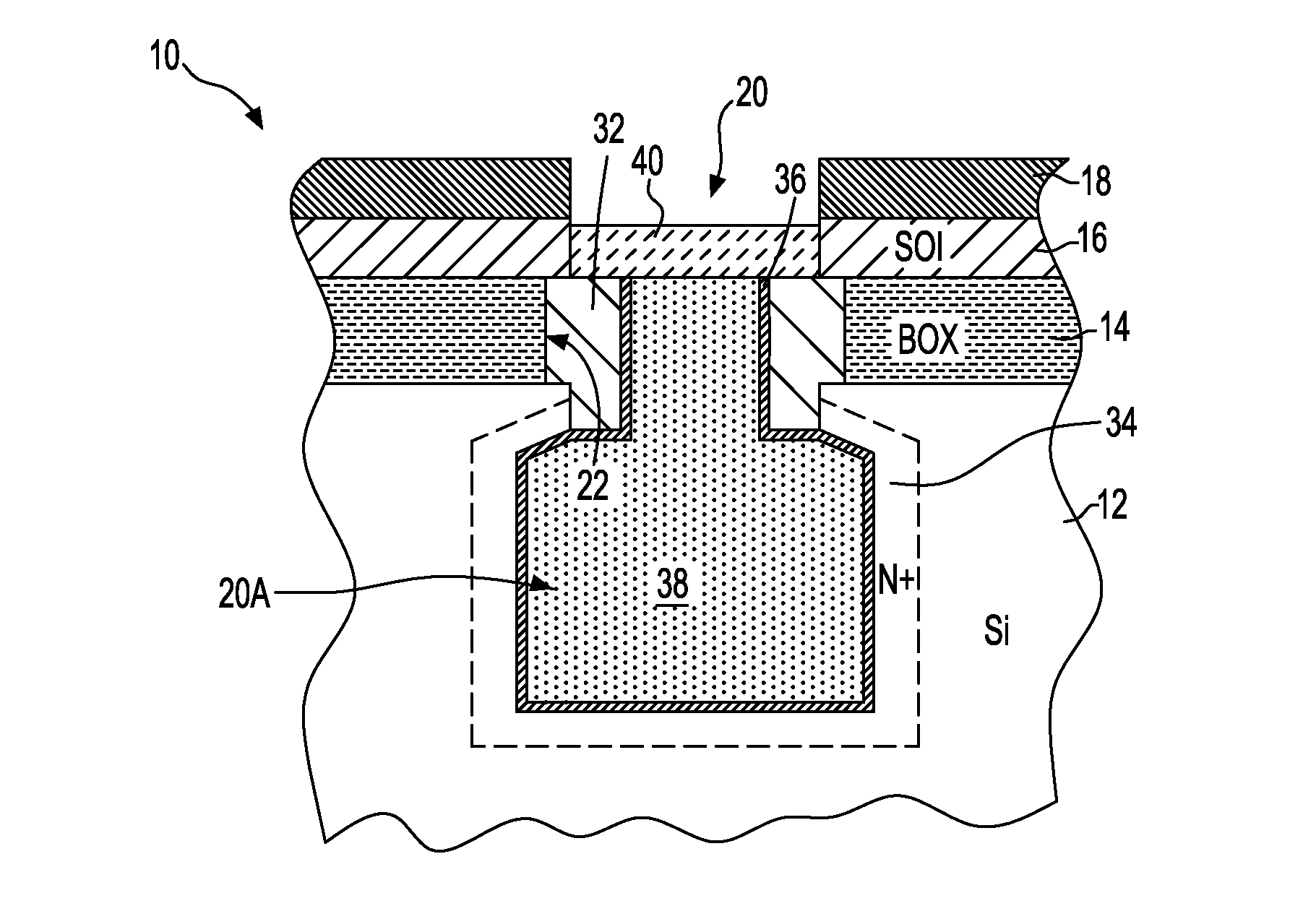
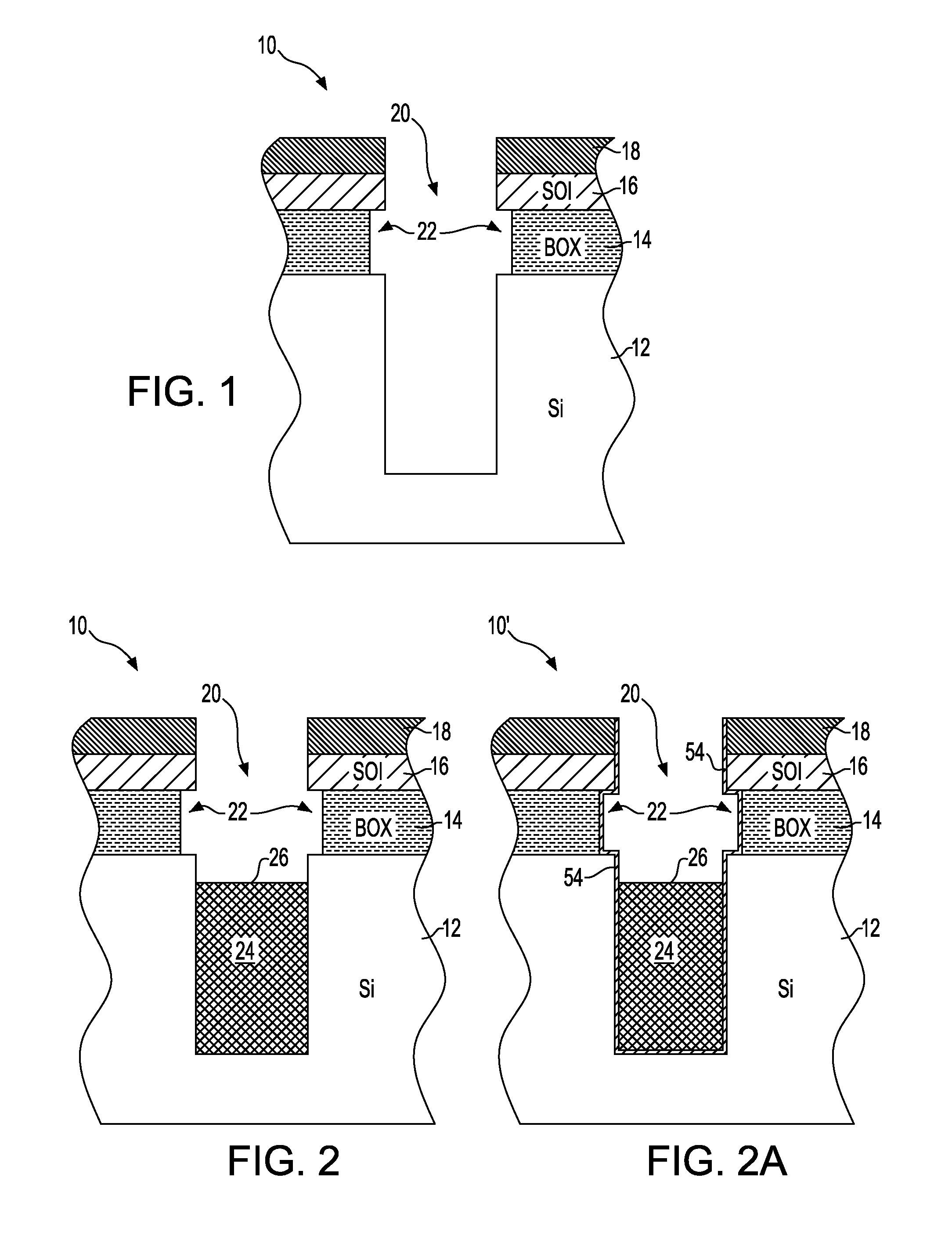
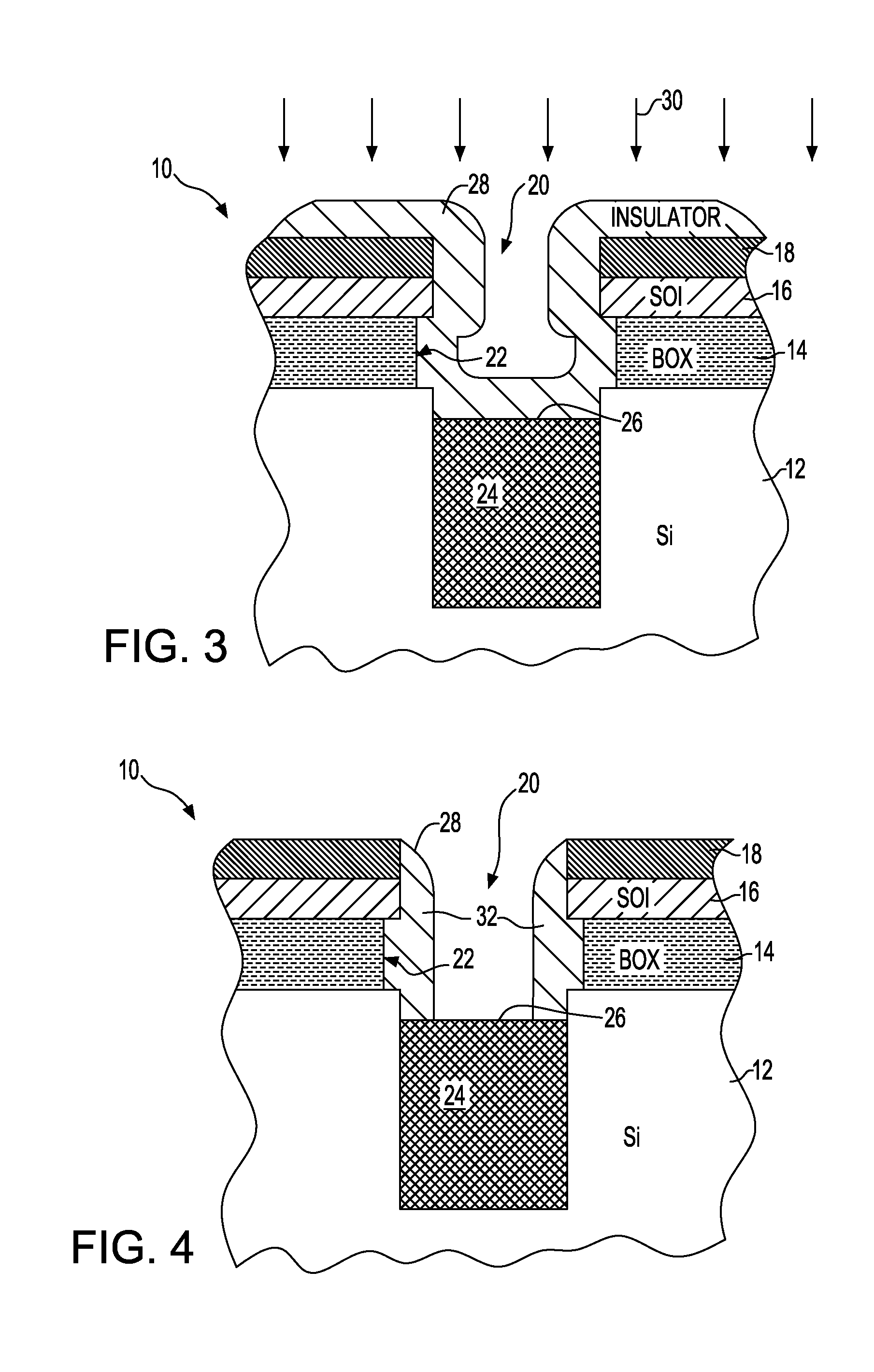
[0032]Referring to the drawings in more detail, and particularly referring to FIG. 1, there is shown a partially fabricated semiconductor structure, most preferably an eDRAM memory cell structure, on a silicon-on-insulator (SOI) substrate 10 which comprises bulk semiconductor layer 12, buried oxide (BOX) layer 14 and SOI layer 16. The bulk semiconductor layer 12 can be any semiconductor material such as silicon, silicon germanium, germanium, a III-V compound semiconductor, or a II-VI compound semiconductor.

[0033]The SOI substrate 10 is fabricated using techniques well known to those skilled in the art. For example, the SOI substrate 10 can be formed by a thermal bonding process, a layer transfer process, or alternatively, the SOI substrate 10 can be formed by an oxygen implantation process, which is referred to in the art as separation by implantation of oxygen (SIMOX).

[0034]The SOI layer 16 is a silicon-containing layer and may include any semiconductor material that includes silic...


PUM


Abstract

A method of forming a silicon-on-insulator (SOI) semiconductor structure in a substrate having a bulk semiconductor layer, a buried oxide (BOX) layer and an SOI layer. During the formation of a trench in the structure, the BOX layer is undercut. The method includes forming a dielectric material on the upper wall of the trench adjacent to the undercutting of the BOX layer and then etching the dielectric material to form a spacer. The spacer fixes the BOX layer undercut and protects it during subsequent steps of forming a bottle-shaped portion of the trench, forming a buried plate in the deep trench; and then forming a trench capacitor. There is also a semiconductor structure, preferably an SOI eDRAM structure, having a spacer which fixes the undercutting in the BOX layer.

Description

BACKGROUND OF THE INVENTION[0001]The present invention relates to electronic devices, and more particularly to semiconductor structures including memory devices, such as eDRAM devices, formed within a silicon-on-insulator (SOI) substrate.[0002]Dynamic Random Access Memory (DRAM) cells are well known. A DRAM cell is essentially a capacitor for storing charge and a pass transistor (also called a pass gate or access transistor) for transferring charge to and from the capacitor. Data stored in the cell is determined by the absence or presence of charge on the storage capacitor. Because cell size affects chip density, and cost, reducing cell area is one of the DRAM designer's primary goals.[0003]One way to accomplish this density goal without sacrificing storage capacitance is to use trench capacitors in the cells. Trench capacitors can be formed by etching deep trenches in a silicon wafer and forming vertically oriented capacitors within each deep trench. Thus, the surface area required...

Claims


Application Information

Patent Timeline
Patent Type & Authority Patents(United States)
IPC IPC(8): H01L27/01H01L27/12H01L31/0392
CPCH01L21/84H01L27/10829H01L27/1087H01L27/1203H10B12/37H10B12/0387
Inventor CHENG, KANGGUOLUSTIG, NAFTALI ELIAHUYANG, DAEWON
Owner INT BUSINESS MASCH CORP
Why Eureka
Try Eureka