Liquid crystal device and projector

a liquid crystal device and projector technology, applied in the field of liquid crystal devices and projectors, can solve the problems of difficult to obtain sufficient brightness, light leakage, and poor display quality when displaying moving images, and achieve the effect of high display quality

Inactive Publication Date: 2011-10-04
SEIKO EPSON CORP
View PDF22 Cites 11 Cited by
  • Summary
  • Abstract
  • Description
  • Claims
  • Application Information

AI Technical Summary

Benefits of technology

[0007]An object of the invention is to provide a liquid crystal device and a projector which are capable of suppressing an aperture ratio from deteriorating due to the presence of a light-shielding film to enable display an image having high brightness and high quality.

Problems solved by technology

Since such light-shielding films can be seen as thin black lines in regions between the projected pixels, surface roughness is increased and thus display quality deteriorates when displaying a moving image.
Since the TFTs are shielded from light by the light-shielding film provided doubly, it can be difficult to obtain sufficient brightness.
Since returning light is prevented by a gate electrode of the TFT used as the switching element, a problem that light leakage occurs due to absence of the light-shielding film on the second substrate does not occur.

Method used


Image

  • Liquid crystal device and projector
  • Liquid crystal device and projector
  • Liquid crystal device and projector

Examples


first embodiment

[0049]First, the configuration of a pixel unit of a liquid crystal device according to a first embodiment of the invention will be described.

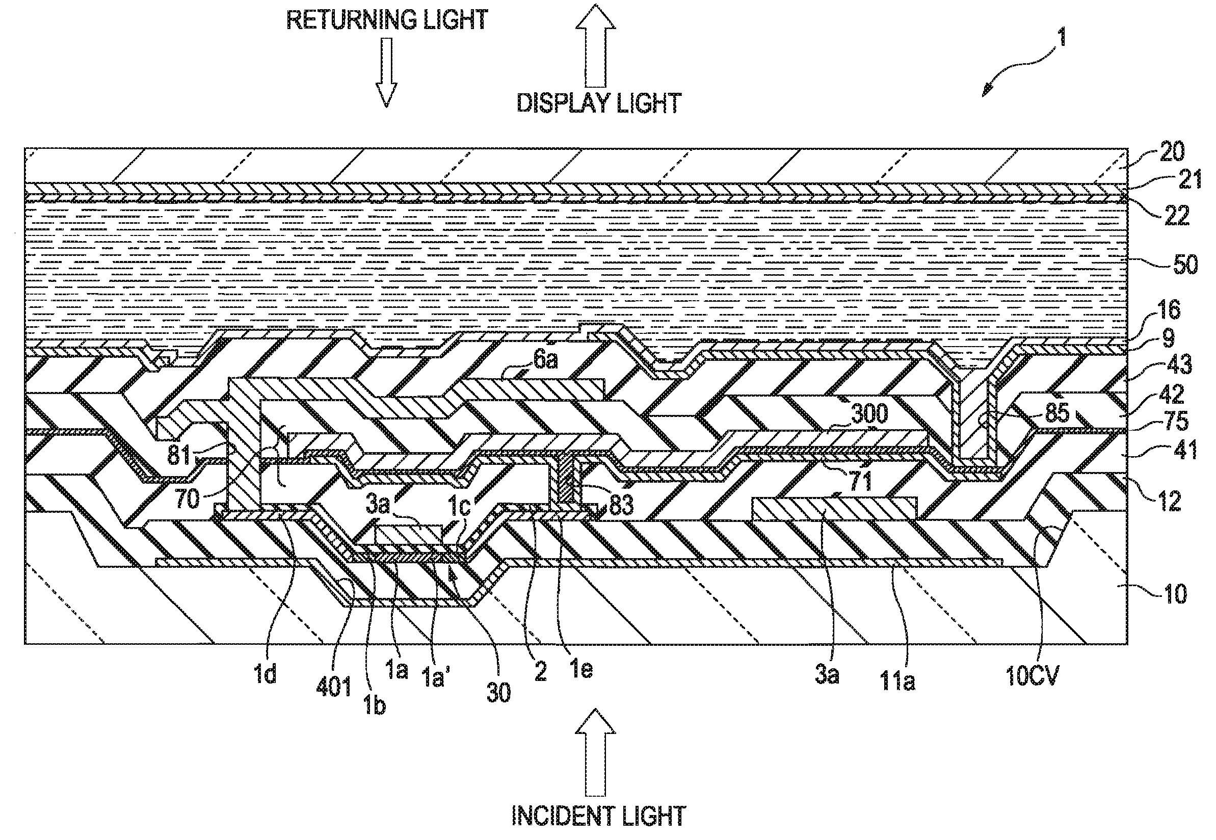
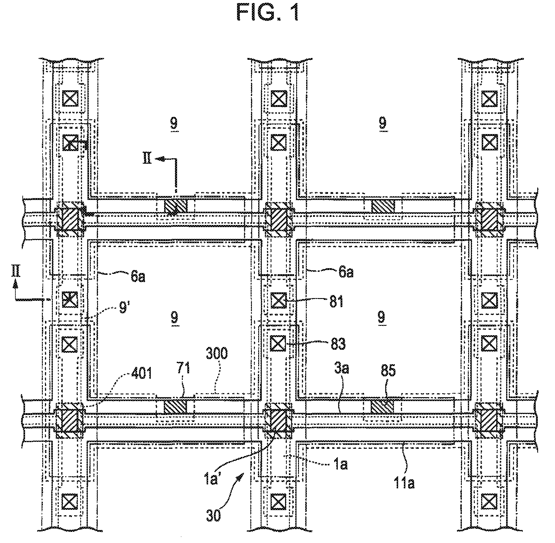
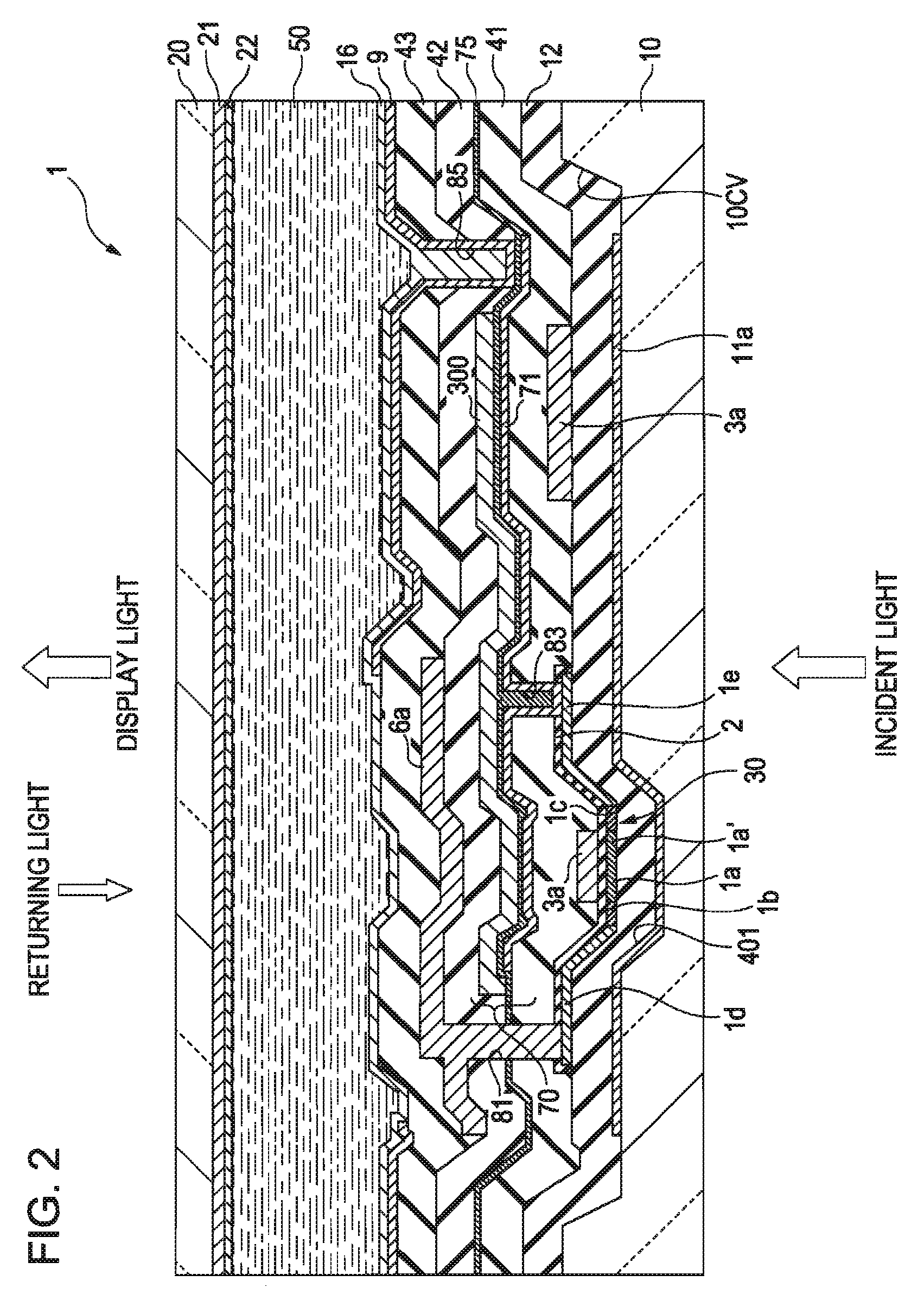
[0050]FIG. 1 is a plan view of a plurality of pixel regions, which are disposed adjacent to one another, on a TFT array substrate on which data lines, scanning lines, and pixel electrodes are formed. FIG. 2 is a cross-sectional view of FIG. 1. In FIG. 2, the scale at which layers and members are drawn is different from that used in FIG. 1 different in order to enable easy recognition of recognize the layers and the members in the drawing.

[0051]As shown in FIG. 2, a plurality of transparent pixel electrodes 9 (indicated by dotted lines 9′) is provided on the TFT array substrate (first substrate) of the liquid crystal device 1 in a matrix and data lines 6a and scanning lines 3a are provided along horizontal and vertical boundaries of the pixel electrodes 9.

[0052]Each of the scanning line 3a faces a channel region 1a′ indicated by minute positive ...

second embodiment

[0087]Next, a liquid crystal device according to a second embodiment of the invention will be described with reference to FIG. 6.

[0088]The basic configuration of the liquid crystal device according to the present embodiment is identical to that of the first embodiment except that a radiation layer 90 is interposed between the TFT 30 and the lower light-shielding film 11a of the TFT array substrate 10. Accordingly, in the present embodiment, the function of the radiation layer will be described using FIG. 6 and the description for the common parts will be omitted.

[0089]The radiation layer 90 is formed on the surface of the lower light-shielding film 11a. As a material of the radiation layer 90, a diamond like carbon (DLC), Al or Ni or the like is suitable and the thickness there of is about 5 nm. The radiation layer 90 has a function for absorbing and radiating heat accumulated in the lower light-shielding film 11a to the outside of the TFT array substrate 10. Accordingly, the heat a...

third embodiment

[0090]Next, a liquid crystal device according to a third embodiment of the invention will be described with reference to FIG. 7.

[0091]The basic configuration of the liquid crystal device according to the present embodiment is identical to that of the first embodiment, except that a microlens which is focusing means is provided at the light incident side of the TFT array substrate 10. Accordingly, in the present embodiment, only the configuration and the operation of the microlens will be described using FIG. 7 and the description or the common parts will be omitted.

[0092]As shown in FIG. 7, a microlens array substrate 110 is provided at the light incident side of the TFT array substrate 10. The microlens array substrate 110 is attached to the upper surface of the TFT array substrate 10 with an adhesive layer 112 interposed therebetween. A plurality of concave curved portions is formed in the microlens array substrate 110 at the side of the TFT array substrate 10 and a microlens 111 ...


PUM

PropertyMeasurementUnit
thicknessaaaaaaaaaa
thicknessaaaaaaaaaa
diameteraaaaaaaaaa

Abstract

Provided is a liquid crystal device including: a plurality of data lines and a plurality of scanning lines which cross each other; switching elements which are provided in correspondence with intersections between the data lines and the scanning lines; pixel electrodes connected to the switching elements; pixels configured in correspondence with the pixel electrodes; an image display region configured by the plurality of pixels; a first substrate having at least the switching elements; a second substrate which faces the first substrate; and liquid crystal interposed between the first substrate and the second substrate, wherein light incident from the first substrate is modulated by the liquid crystal, a light-shielding film is provided on a light incident side of at least the switching elements of the first substrate, and at least a portion corresponding to the image display region of the second substrate includes only a transparent layer which transmits light incident to the liquid crystal.

Description

BACKGROUND[0001]1. Technical Field[0002]The present invention relates to a liquid crystal device and a projector.[0003]2. Related Art[0004]Projectors have come into widespread use in homes. Accordingly, a spatial light modulation device of a projector having low cost, long life span and capable of producing images of high brightness is desired to be obtained. A representative example of the spatial light modulation device is a liquid crystal device. A known example of a liquid crystal display is an active matrix type liquid crystal device having thin-film transistors TFTs as pixel switching elements. In this liquid crystal device, when light is irradiated onto a channel region of the TFT provided in each of a plurality of pixels provided in the liquid crystal device, a light leakage current occurs due to excitation by the light and thus the characteristics of the TFT are changed. Accordingly, the TFTs are protected by light-shielding films provided on a TFT array substrate and an op...

Claims


Application Information

Patent Timeline
Patent Type & Authority Patents(United States)
IPC IPC(8): G02F1/1335G02F1/1368G02F1/133
CPCG02F1/136209G09G3/3611H04N9/3105H04N9/3197G02F1/133526G02F2001/133567G02F2201/40G09G3/2092G09G3/3614G09G3/3674G09G2310/0205G09G2360/18G02F1/133567G02F1/13G02F1/1335
Inventor KAMIJIMA, SHINJI
Owner SEIKO EPSON CORP
Why Eureka
Try Eureka