
Nitride semiconductor heterojunction field effect transistor having wide band gap barrier layer that includes high concentration impurity region

a heterojunction field effect and semiconductor technology, applied in the field of semiconductor heterojunction field effect transistors, can solve the problems of inability to obtain desired output, difficulty in forming source/drain (ohmic) even more difficulty in forming source/drain electrodes with low resistance, etc., to achieve high breakdown voltage, high output, and high output.

Inactive Publication Date: 2011-10-11
MITSUBISHI ELECTRIC CORP
View PDF9 Cites 14 Cited by
  • Summary
  • Abstract
  • Description
  • Claims
  • Application Information

AI Technical Summary

Benefits of technology

[0008]The objective of the present invention is to provide a semiconductor device of a hetero-junction field effect transistor that is capable of obtaining a high output and a high breakdown voltage, and a manufacturing method of the same. Further, the objective of the present invention is to provide a hetero-junction field effect transistor consisting of a nitride semiconductor that is capable of realizing of a source / drain (ohmic) electrode with low resistance even when a nitride semiconductor having a large band gap is used.
[0012]Because the manufacturing method of a semiconductor device according to one embodiment of the present invention includes a step of forming an AlxGa1-xN (0<x<1) channel layer with a larger electric breakdown field and a larger band gap than that of GaN, it can manufacture a semiconductor device of a hetero-junction field effect transistor that is capable of obtaining a high output and a high breakdown voltage.
[0014]The semiconductor device according to one embodiment of the present invention can reduce the ohmic contact resistance, and therefore it can realize a device having a large current and a high output.

Problems solved by technology

However, a desired output cannot be obtained in the conventional hetero-junction field effect transistor consisting of a nitride semiconductor, and it is necessary to make it have a higher output.
However, because the higher the electric breakdown field the material has, the larger the band gap is, and on the contrary, a source / drain (ohmic) electrode having low resistance is difficult to form.
Especially in the case of the hetero-junction field effect transistor, because it is necessary that the material used in the barrier layer has a larger band gap than that of the channel layer, when the material used in the channel layer has a large band gap, it becomes larger than the band gap of the material used in a barrier layer, and a source / drain (ohmic) electrode having low resistance is even more difficult to form.

Method used


Image

  • Nitride semiconductor heterojunction field effect transistor having wide band gap barrier layer that includes high concentration impurity region
  • Nitride semiconductor heterojunction field effect transistor having wide band gap barrier layer that includes high concentration impurity region
  • Nitride semiconductor heterojunction field effect transistor having wide band gap barrier layer that includes high concentration impurity region

Examples


embodiment 1

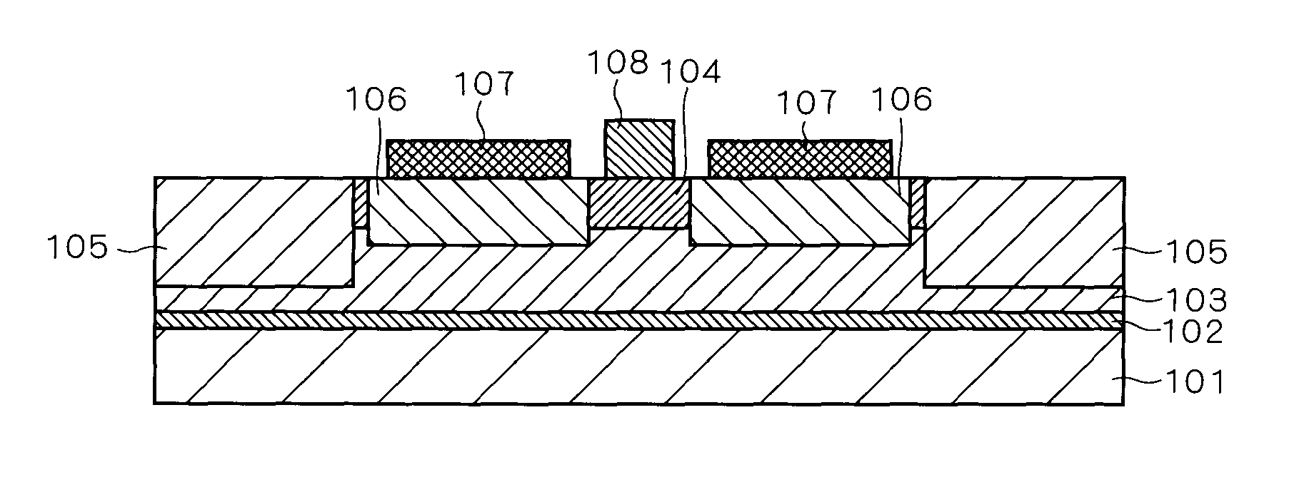
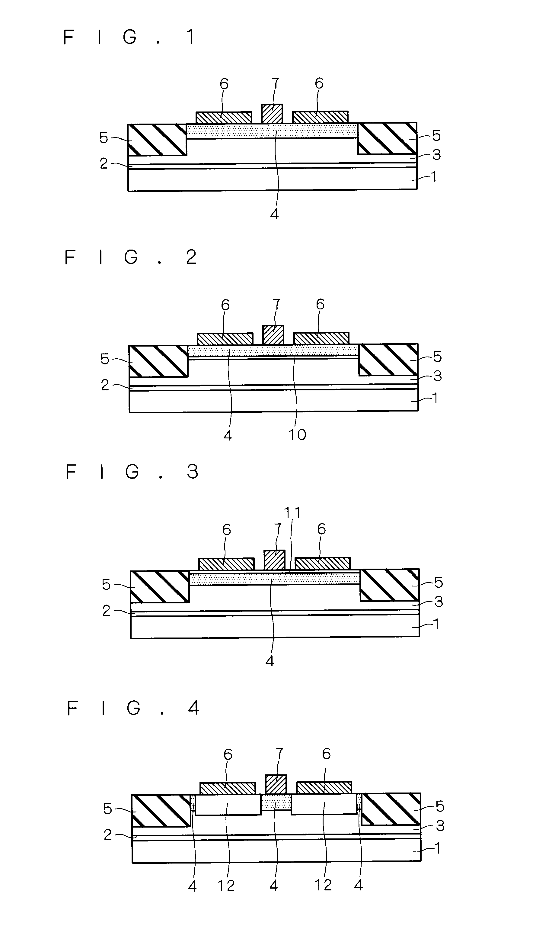
[0044]FIG. 1 is a cross-sectional drawing of the hetero-junction field effect transistor according to the embodiment of the present invention. In the hetero-junction field effect transistor shown in FIG. 1, a semi-insulated SiC substrate 1 is provided in the lowest layer, and a channel layer 3 of 1 μm thickness, consisting of Al0.6Ga0.4N, is provided on top of it via a buffer layer 2. Further, in the hetero-junction field effect transistor shown in FIG. 1, a barrier layer 4 of 10 nm thickness, consisting of AlN, forms a hetero-junction with the channel layer 3. Further, in the hetero-junction field effect transistor shown in FIG. 1, an element separation region 5 is provided in the regions on both sides in the drawing, and source / drain electrodes 6 consisting of Ti / Al and a gate electrode 7 consisting of Ni / Au are provided on the barrier layer 4.

[0045]The off breakdown voltage of the hetero-junction field effect transistor depends on the electric breakdown field of the channel layer...

embodiment 2

[0064]The calculation result of the energy band structure (energy (eV)) and the carrier concentration (cm−3) in the depth direction of the barrier layer 4 and the channel layer 3 of the hetero-junction field effect transistor shown in FIG. 1 is shown in FIG. 9. The calculation result is obtained by solving Poisson's equation and Schrödinger's equation self-consistently. Moreover, values that are generally used are used as physical property values used in the above-described calculation.

[0065]In the graph shown in FIG. 9, the value in which the carrier concentration is integrated with the depth direction is made to be the sheet carrier density (Ns), and the sheet carrier density of the hetero-junction field effect transistor shown in FIG. 1 is obtained to be 1.6×10¹³ (cm−2).

[0066]Similarly, the relationship of the sheet carrier density (cm−2) and the thickness (t) (nm) of the barrier layer 4 in the case of combining the Al composition ratio x of the channel layer 3 and the Al composi...

embodiment 3

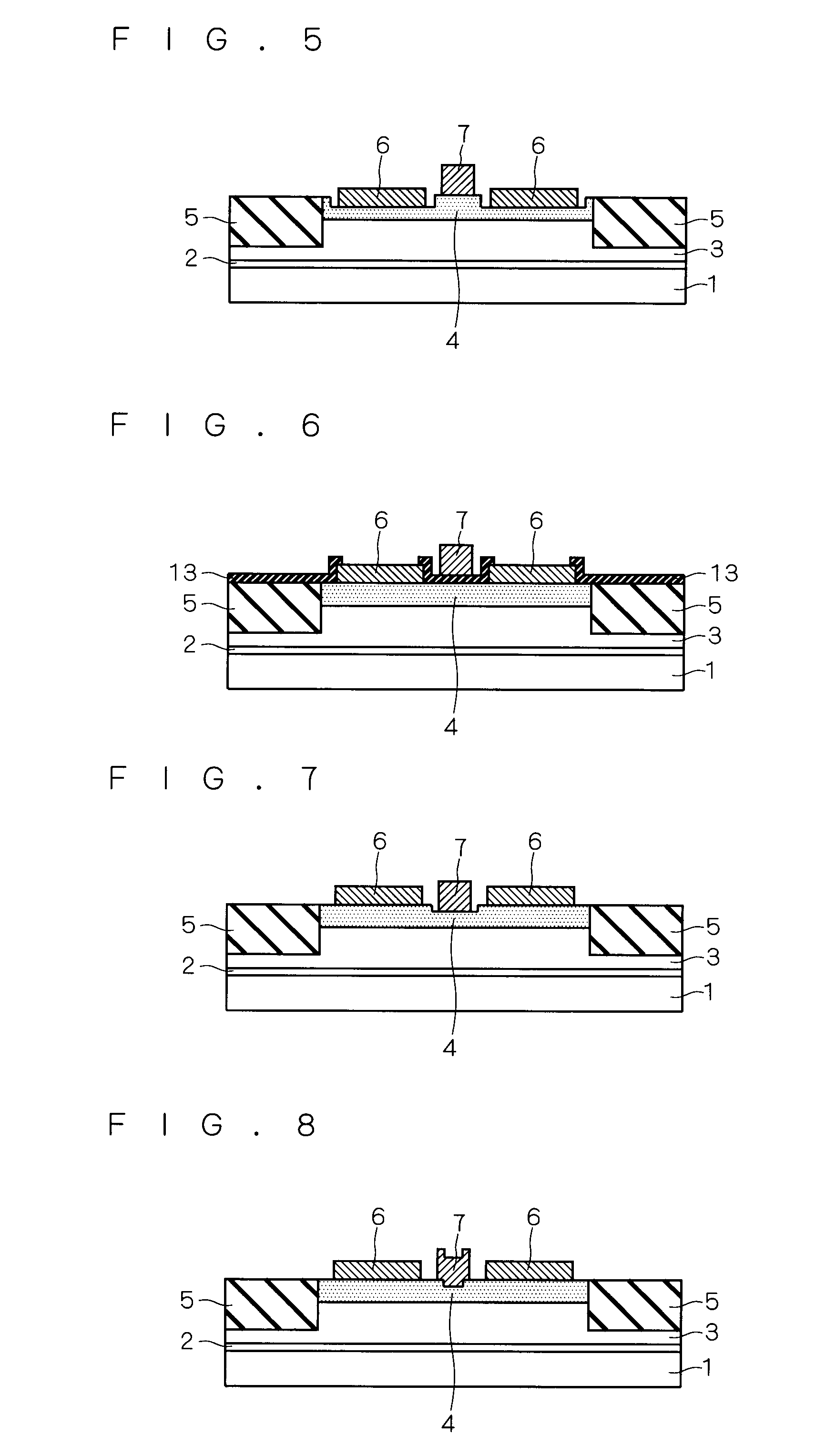
[0079]A manufacturing process of the hetero-junction field effect transistor shown in FIG. 1 is shown in FIGS. 15 to 18. Moreover, the same reference numbers are appended to the constituting elements in FIGS. 15 to 18 that are the same constituting elements shown in FIG. 1, and detailed explanation is omitted. First, with respect to FIG. 15, the buffer layer 2, the channel layer 3 consisting of Al0.6Ga0.4N, and the barrier layer 4 consisting of AlN are epitaxial grown in order by applying an epitaxial growth method such as a MOCVD (Metal Organic Chemical Vapor Deposition) method and a MBE (Molecular Beam Epitaxy) method on the SiC substrate 1.

[0080]Next, with respect to FIG. 16, a metal layer such as Ti, Al, Ni, Ta, Au, Mo, and W is deposited by using a vapor deposition method or a sputter method, and the source / drain electrodes 6 are formed with a lift-off method, etc.

[0081]Next, with respect to FIG. 17, the element separation region 5 is formed in the channel layer 3 and the barri...


PUM


Abstract

The objective of the present invention is to provide a semiconductor device of a hetero-junction field effect transistor that is capable of obtaining a high output and a high breakdown voltage and a manufacturing method of the same. The present invention is a semiconductor device of a hetero-junction field effect transistor provided with an AlxGa1-xN channel layer with a composition ratio of Al being x (0<x<1) formed on a substrate, an AlyGa1-yN barrier layer with a composition of Al being y (0<y≦1) formed on the channel layer, and source / drain electrodes and a gate electrode formed on the barrier layer, wherein the composition ratio y is larger than the composition ratio x.

Description

BACKGROUND OF THE INVENTION[0001]1. Field of the Invention[0002]The present invention is an invention relating to a semiconductor device and a manufacturing method of the same, and especially relating to a semiconductor device of a hetero-junction field effect transistor and a manufacturing method of the same.[0003]2. Description of the Background Art[0004]A GaN layer is used as a channel layer in a conventional hetero-junction field effect transistor of a semiconductor device containing nitride. A specific configuration is disclosed in Yasuhiro Okamoto and 5 others, “L-Band High Output AlGaN / GaN Hetero-junction FET on SiC Substrate”, Technical Report of IEICE, The Institute of Electronics, Information and Communication Engineers, 2002, ED2002-94, pp. 85-88. An L-band high output AlGaN / GaN hetero-junction FET on a SiC substrate is disclosed in Yasuhiro Okamoto and 5 others, “L-Band High Output AlGaN / GaN Hetero-junction FET on SiC Substrate”, Technical Report of IEICE, The Institute ...

Claims


Application Information

Patent Timeline
Patent Type & Authority Patents(United States)
IPC IPC(8): H01L29/778
CPCH01L29/2003H01L29/432H01L29/66462H01L29/7783H01L29/7786H01L29/802H01L29/4175H01L29/42316
Inventor NANJO, TAKUMASUITA, MUNEYOSHIABE, YUJIOISHI, TOSHIYUKITOKUDA, YASUNORI
Owner MITSUBISHI ELECTRIC CORP
Learn More