Semiconductor memory device and control method thereof

a memory device and semiconductor technology, applied in the direction of information storage, static storage, digital storage, etc., can solve the problems of complicated control by a controller, inconvenient storage of drams, and limit to lowering power consumption, so as to avoid data destruction, avoid data destruction, and secure compatibility with drams

Inactive Publication Date: 2011-10-11
LONGITUDE LICENSING LTD
View PDF18 Cites 5 Cited by
  • Summary
  • Abstract
  • Description
  • Claims
  • Application Information

AI Technical Summary

Benefits of technology

[0016]According to the present invention, a plurality of sense amplifiers, which can be connected to any of a plurality of bit lines, are provided, and thus it becomes possible to execute a read operation for a plurality of memory cells connected to the same word line in parallel. Accordingly, even when the sensing operation takes a long period of time, the data reading can be performed at high speed by a parallel operation.
[0017]Furthermore, when the read operation is consecutively requested to the same memory cell, starting of the sense amplifier is stopped temporarily by an address determining circuit, and thus the sense amplifiers are not operated for the same memory cell in parallel. Accordingly, it becomes possible to avoid a data destruction occurring as a result of the sense amplifiers being operated for the same memory cell in parallel.
[0018]As a result, a high-speed read operation can be performed on an arbitrary address, and thus, even when the present invention is targeted for a PRAM, for example, the compatibility with a DRAM can be secured.

Problems solved by technology

However, DRAM is a volatile memory, and therefore there are problems as follows.
Stored data is lost once the power supply is disconnected, and thus DRAM is not suitable for storing a program or archival data that should be saved for a long period of time.
Further, even when the power supply is being inputted, a periodic refreshing operation needs to be performed to maintain the data, and thus there is a limit to lowering of power consumption and also complicated control by a controller is necessary.
However, even in the flash memory, there are disadvantages such that a large current is necessary for writing or deleting data, and also it requires a very long time for writing and erasing data.
Therefore, it is not appropriate to use flash memory as an alternative to DRAM as a main memory.
In addition, non-volatile memories such as MRAM (Magnetoresistive Random Access Memory) and FRAM (Ferroelectric Random Access Memory) have been proposed; however, these memories have a difficulty in obtaining the memory capacity equivalent to that of DRAM.
Accordingly, it is not practical to arrange the sense amplifier for each bit line like DRAM, and this requires sharing the same sense amplifier for a plurality of bit lines.
As a result, a data reading cycle is restricted by an operation speed of the sense amplifier.
Hence, it has a problem that the data reading cycle becomes much longer as compared to that of the DRAM, which in turn cannot keep the compatibility with the DRAM.
Such a problem similarly occurs not only in PRAM but also in semiconductor memory devices of other types (for example, RRAM: Resistive Random Access Memory), in which a sensing operation takes a long period of time.

Method used


Image

  • Semiconductor memory device and control method thereof
  • Semiconductor memory device and control method thereof
  • Semiconductor memory device and control method thereof

Examples


Embodiment Construction

[0031]Preferred embodiments of the present invention will be explained below in detail with reference to the accompanying drawings.

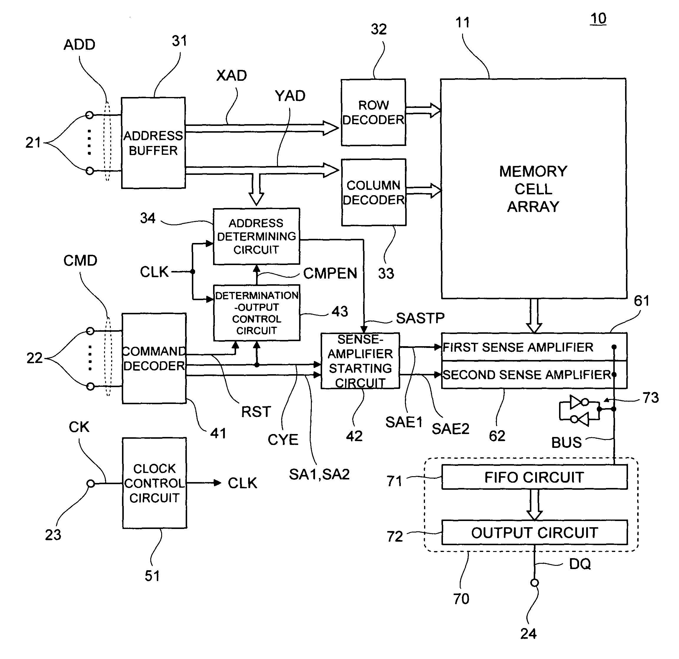
[0032]FIG. 1 is a block diagram showing a configuration of a semiconductor memory device according to a preferred embodiment of the present invention.

[0033]As shown in FIG. 1, a semiconductor memory device 10 according to the present embodiment includes a memory cell array 11 including a plurality of memory cells MC, a plurality of address terminals 21 that receive an address signal ADD, a plurality of command terminals 22 that receive a command signal CMD, a clock terminal 23 that receives an external clock signal CK, and a data terminal 24 that inputs and outputs data DQ. Although not particularly limited, the semiconductor memory device 10 is of a synchronous type which operates in synchronization with the external clock signal CK.

[0034]The address signal ADD inputted via the address terminals 21 is supplied to an address buffer 31. Among the address ...


PUM


Abstract

A semiconductor memory device (and control method therefor) includes a plurality of word lines, a plurality of bit lines, a plurality of memory cells arranged at intersections of the word lines and the bit lines, a word driver that selects any one of the word lines, a plurality of sense amplifiers connectable to any of the bit lines, a sense-amplifier starting circuit that sequentially starts the sense amplifiers in response to a request of consecutive read operations to the memory cells connected to a predetermined word line, in a state that the predetermined word line is selected by the word driver, and an address determining circuit that temporarily stops an operation of the sense-amplifier starting circuit in response to a request of consecutive read operations to a same memory cell connected to a predetermined word line, in a state that the predetermined word line is selected by the word driver.

Description

BACKGROUND OF THE INVENTION[0001]1. Field of the Invention[0002]The present invention relates to a semiconductor memory device and a control method thereof, and particularly relates to a semiconductor memory device including a plurality of sense amplifiers that can be connected to any of a plurality of bit lines and a control method thereof.[0003]2. Description of Related Art[0004]Currently, there are various types of semiconductor memory devices, and DRAM (Dynamic Random Access Memory) can be mentioned as a representative thereof. Most of DRAMs are of a synchronous type in which data is inputted and outputted in synchronization with a clock signal, and can be randomly accessed with a cycle of about 7 ns.[0005]However, DRAM is a volatile memory, and therefore there are problems as follows. Stored data is lost once the power supply is disconnected, and thus DRAM is not suitable for storing a program or archival data that should be saved for a long period of time. Further, even when t...

Claims


Application Information

Patent Timeline
Patent Type & Authority Patents(United States)
IPC IPC(8): G11C7/00
CPCG11C7/06G11C7/22G11C8/08G11C13/0004G11C13/0028G11C13/004G11C13/0061G11C13/0023G11C2213/79G11C2013/0054
Inventor MAE, KENJI
Owner LONGITUDE LICENSING LTD
Why Eureka
Try Eureka