Electronic circuit arrangement

a technology of electronic circuit and arrangement, applied in the direction of semiconductor devices, semiconductor/solid-state device details, electrical apparatus, etc., can solve the problems of inability, disadvantage of both variants, and only to a very limited extent, and achieve the effect of cost-effective production and uniformity

Active Publication Date: 2011-10-18
INFINEON TECH AG
View PDF23 Cites 4 Cited by
  • Summary
  • Abstract
  • Description
  • Claims
  • Application Information

AI Technical Summary

Benefits of technology

[0014]Preferably, the soldering layer is lead-free. The soldering layer is therefore nontoxic and ecologically safe and can be processed without particular protective precautions.
[0020]Preferably, a surface of the chip carrier is provided with a soldering layer essentially over the whole area. That is to say that at least one side of the substrate is coated with the soldering layer uniformly and over the whole area. Consequently, the chip carrier can be produced uniformly. A complicated procedure for differing coating of the chip carrier is obviated. The production of the chip carrier can be configured in cost-effective and efficient fashion.

Problems solved by technology

This is not possible, or is possible only to a very limited extent, in the case of wire bonding because wires would then cross one another and very probably make contact with one another.
Both variants have disadvantages, however.
Tin-plated chip carriers tend to form so-called whiskers, acicular elongate crystals, which can lead to short circuits when the circuit arrangement is mounted on printed circuit boards.
These soldering layers have the disadvantage, however, that eutectic bonding with metalized chips, for example, by means of an AuSn or AuAs alloy, is not possible.
This is particularly problematic since stringent requirements with regard to reliability, stability and also thermal and electrical conductivity are made of the connection of the chip to the chip carrier.

Method used


Image

  • Electronic circuit arrangement
  • Electronic circuit arrangement
  • Electronic circuit arrangement

Examples


Embodiment Construction

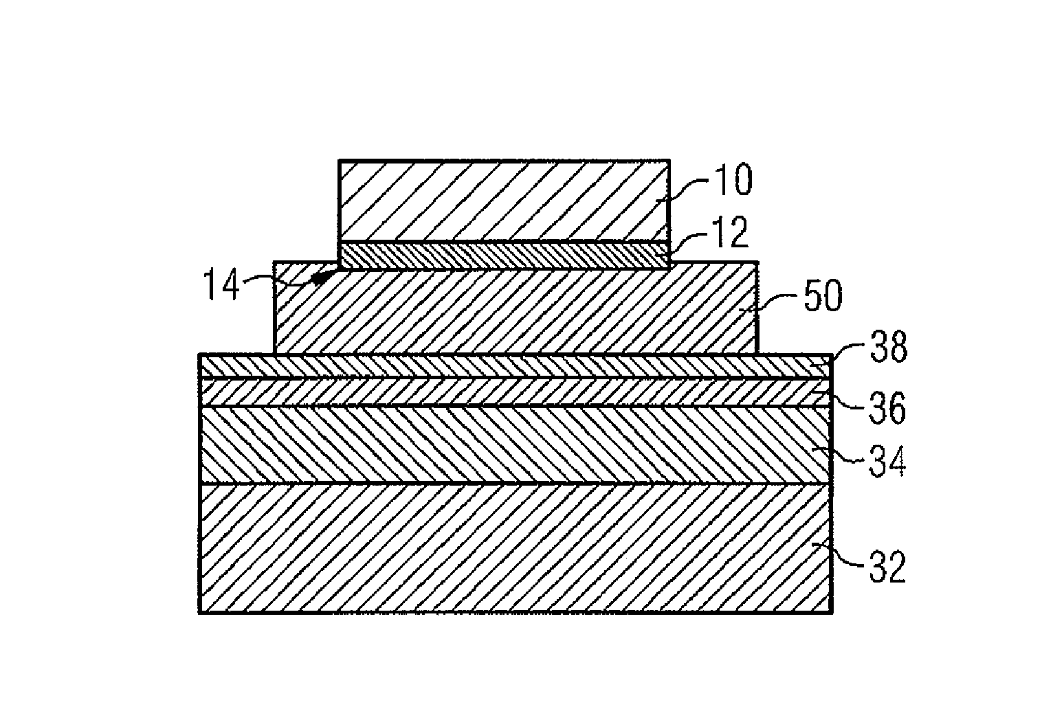
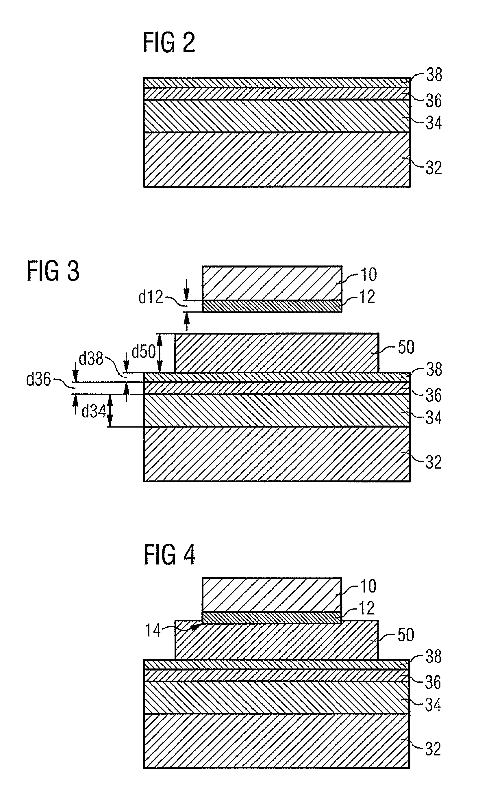
[0034]In the description below, the same reference numerals are used for identical and identically acting parts.

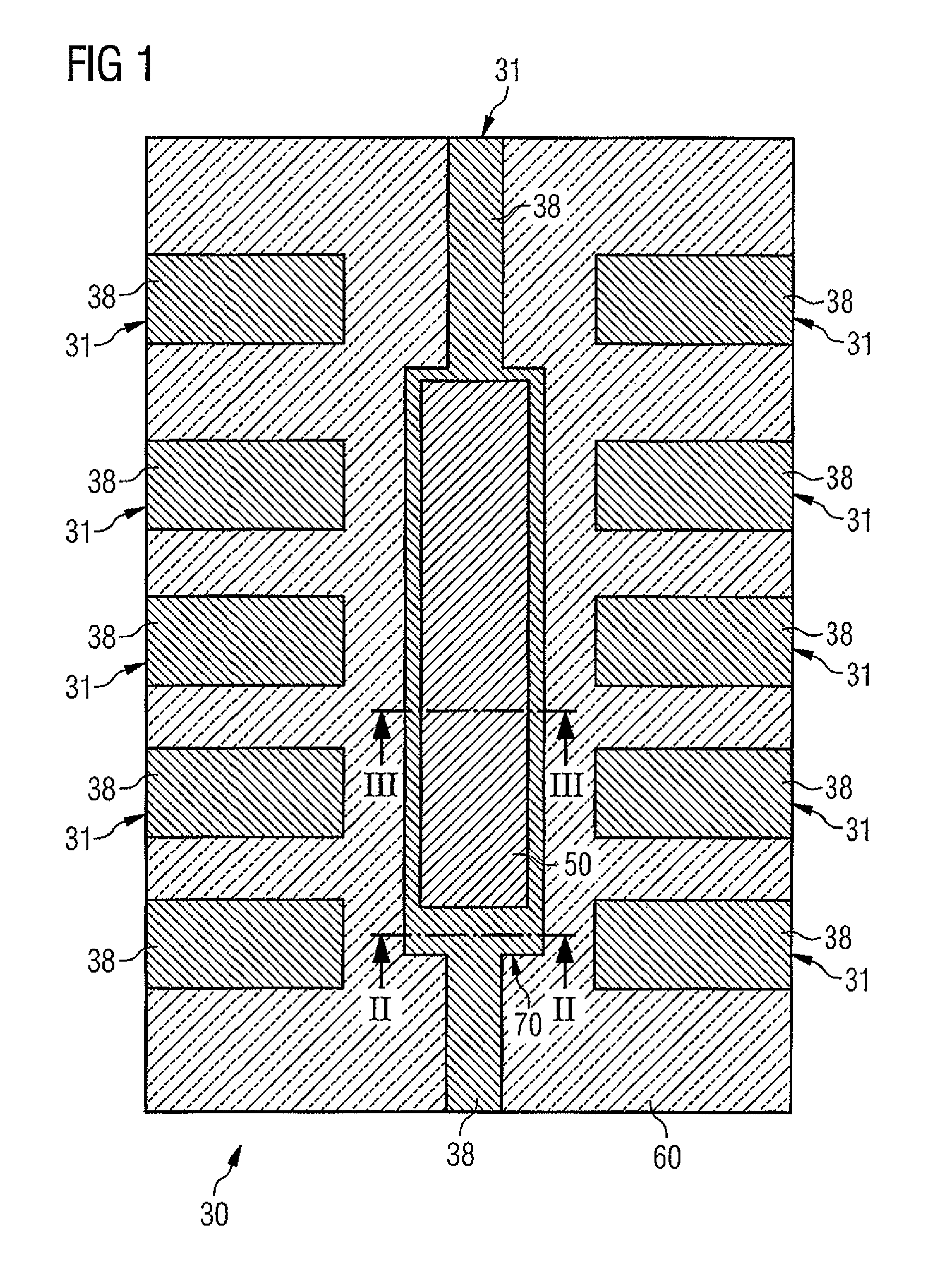
[0035]FIG. 1 shows a schematic plan view of a first embodiment chip carrier 30. The chip carrier 30 preferably is formed essentially in rectangular fashion and has at its edges a plurality of contact regions 31 serving, for a silicon chip 10 (see FIG. 3) applied on the carrier layer 30 later, as connection pieces for further processing. For this purpose, the silicon chip 10 is connected to the contact regions 31 of the chip carrier 30, for example, by means of a fine wiring. Extending centrally along the longitudinal direction of the chip carrier 30 is a web with a rectangular widening, the so-called chip contact location 70, on which the chip 10 is fixed in a further processing step.

[0036]The lateral contact regions 31 and also the chip contact location 70 are separated from one another by an intermediate region 60. In a later method step, the intermediate region 60 can b...


PUM


Abstract

Electronic circuit arrangement, includes a chip and a chip carrier having a substrate and a chip contact location. At least the chip contact location is provided with a soldering layer. The chip includes a bonding layer. A silver layer for eutectic bonding with the bonding layer is provided on the soldering layer in the region of the chip contact location.

Description

[0001]This application claims priority to German Patent Application 10 2006 023 998.9, which was filed May 22, 2006, and is incorporated herein by reference.TECHNICAL FIELD[0002]The invention relates to an electronic circuit arrangement and also to a method for producing it.BACKGROUND[0003]An electronic circuit arrangement can include a semiconductor chip and a chip carrier, which are at least partly packaged in a housing (so-called packaging). The chip carrier for the at least one semiconductor chip has a plurality of functions in a finished package. It serves as a stable bearing and holding area to which the semiconductor chip is fixedly connected, dissipates heat that arises, and provides the electrical connections for the semiconductor chip. That is to say that it forms the contact elements for the electronic circuit arrangement which are connected to printed circuit boards, for example, in a further processing step.[0004]The semiconductor chip is usually connected to a chip con...

Claims


Application Information

Patent Timeline
Patent Type & Authority Patents(United States)
IPC IPC(8): H01L23/48
CPCH01L24/29H01L24/83H01L24/32H01L2224/29144H01L2224/32506H01L2224/83193H01L2224/83201H01L2224/83801H01L2924/01005H01L2924/0102H01L2924/01029H01L2924/01046H01L2924/01047H01L2924/0105H01L2924/01079H01L2924/01082H01L2924/01322H01L2924/01033H01L2924/01006H01L2924/01068H01L2924/014H01L2224/29101H01L2924/00H01L2924/0132H01L2924/0133H01L2924/01026H01L2924/01028H01L2924/15747H01L2224/29111H01L2924/00014H01L2924/00015H01L2924/10253
Inventor HOSSEINI, KHALILMAHLER, JOACHIM
Owner INFINEON TECH AG
Why Eureka
Try Eureka