Semiconductor device employing group III-V nitride semiconductors and method for manufacturing the same

a technology of nitride semiconductors and semiconductors, applied in the direction of semiconductor devices, basic electric elements, electrical appliances, etc., can solve the problems of reducing resistance and improving speed of silicon devices, and becoming difficult to meet market requirements, and achieves high breakdown voltage, high current, and easy feeding

Active Publication Date: 2011-10-25
ROHM CO LTD
View PDF13 Cites 40 Cited by
  • Summary
  • Abstract
  • Description
  • Claims
  • Application Information

AI Technical Summary

Benefits of technology

[0015]According to this structure, the first electrode portion in contact with the P-type group III-V nitride semiconductor layer is constituted of the first conductive material, and the second electrode portion in contact with the N-type group III-V nitride semiconductor layer is constituted of the second conductive material. Therefore, an electrode constituted by bonding the first and second electrode portions to each other can be excellently brought into contact (ohmic contact) with the P-type and N-type group III-V nitride semiconductor layers at the same time by properly selecting the first and second conductive materials.
[0058]The gate insulating film may include a group III-V nitride intrinsic semiconductor gate layer (51: regrowth layer) containing Al (preferably containing no In). According to this structure, the group III-V nitride intrinsic semiconductor gate layer containing Al forms an excellent interface between the same and the wall surface of the first to third group III-V nitride semiconductor layers. Therefore, such inconveniences that the carrier mobility in the channel region lowers and the reliability of the device lowers due to an unstable interface can be avoided dissimilarly to a case of forming an insulating film such as an oxide film in contact with the wall surface of the first to third group III-V nitride semiconductor layers.

Problems solved by technology

However, improvement in breakdown voltage, reduction in resistance and improvement in speed of a silicon device are now reaching limits due to the theoretical limit of the silicon semiconductor, and it is becoming difficult to satisfy requirements of the market.

Method used


Image

  • Semiconductor device employing group III-V nitride semiconductors and method for manufacturing the same
  • Semiconductor device employing group III-V nitride semiconductors and method for manufacturing the same
  • Semiconductor device employing group III-V nitride semiconductors and method for manufacturing the same

Examples


first embodiment

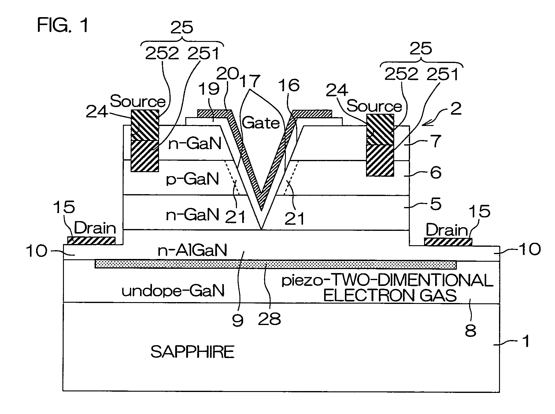
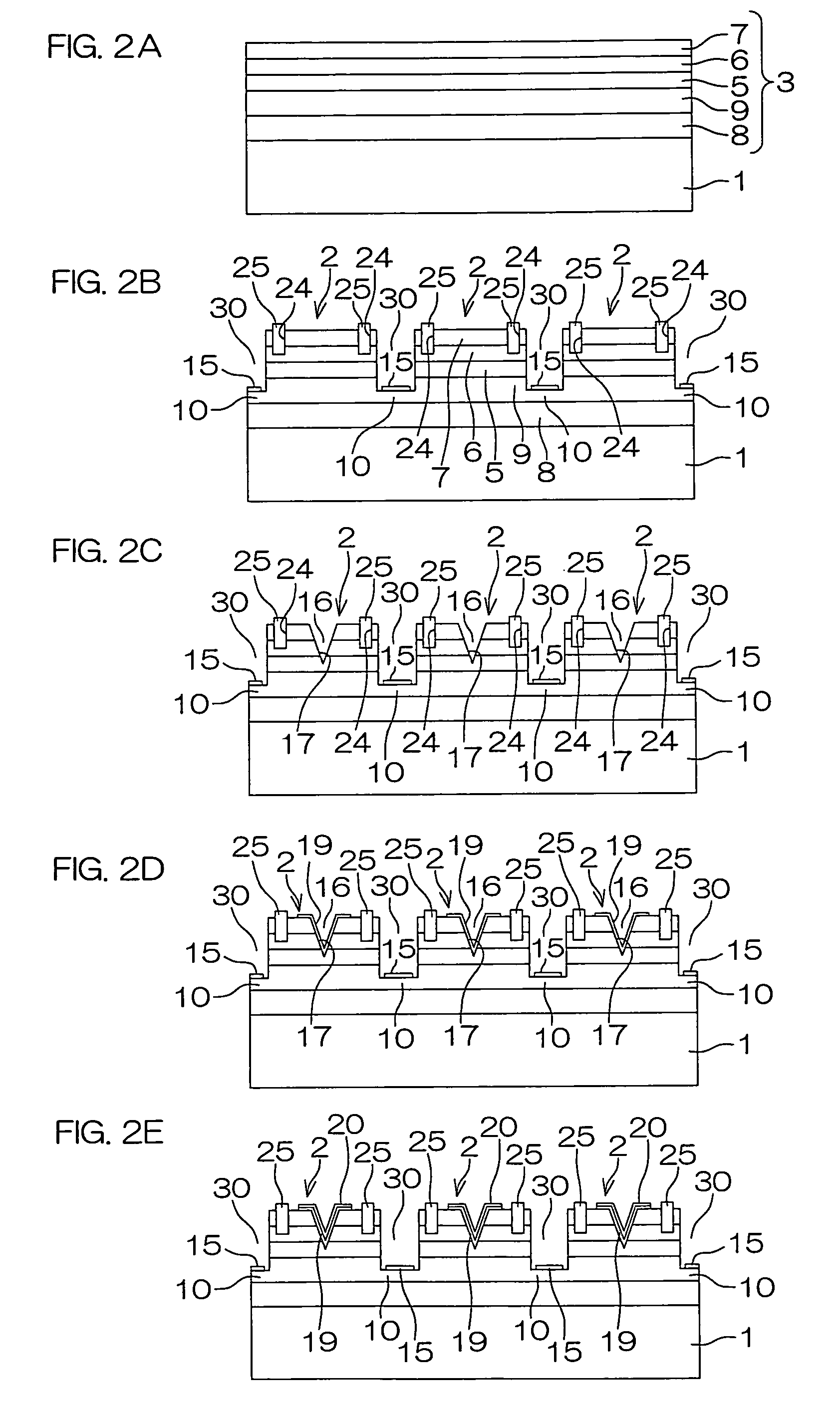
[0079]FIG. 1 is a schematic sectional view for illustrating the structure of an MIS field-effect transistor according to the present invention. This field-effect transistor includes a sapphire substrate 1 which is an insulating substrate and a nitride semiconductor multilayer structure portion 2 consisting of GaN compound semiconductor layers grown on this sapphire substrate 1. The nitride semiconductor multilayer structure portion 2 includes an N-type GaN layer 5 (drain layer), a P-type GaN layer 6 stacked on this N-type GaN layer 5 and an N-type GaN layer 7 (source layer) stacked on this P-type GaN layer 6. Further, the nitride semiconductor multilayer structure portion 2 includes an intrinsic (undoped) GaN layer 8 formed in contact with the sapphire substrate 1 and an N-type AlGaN layer 9 stacked on this intrinsic GaN layer 8, and the N-type GaN layer 5 is stacked on this N-type AlGaN layer 9.

[0080]The nitride semiconductor multilayer structure portion 2 is etched up to such a de...

second embodiment

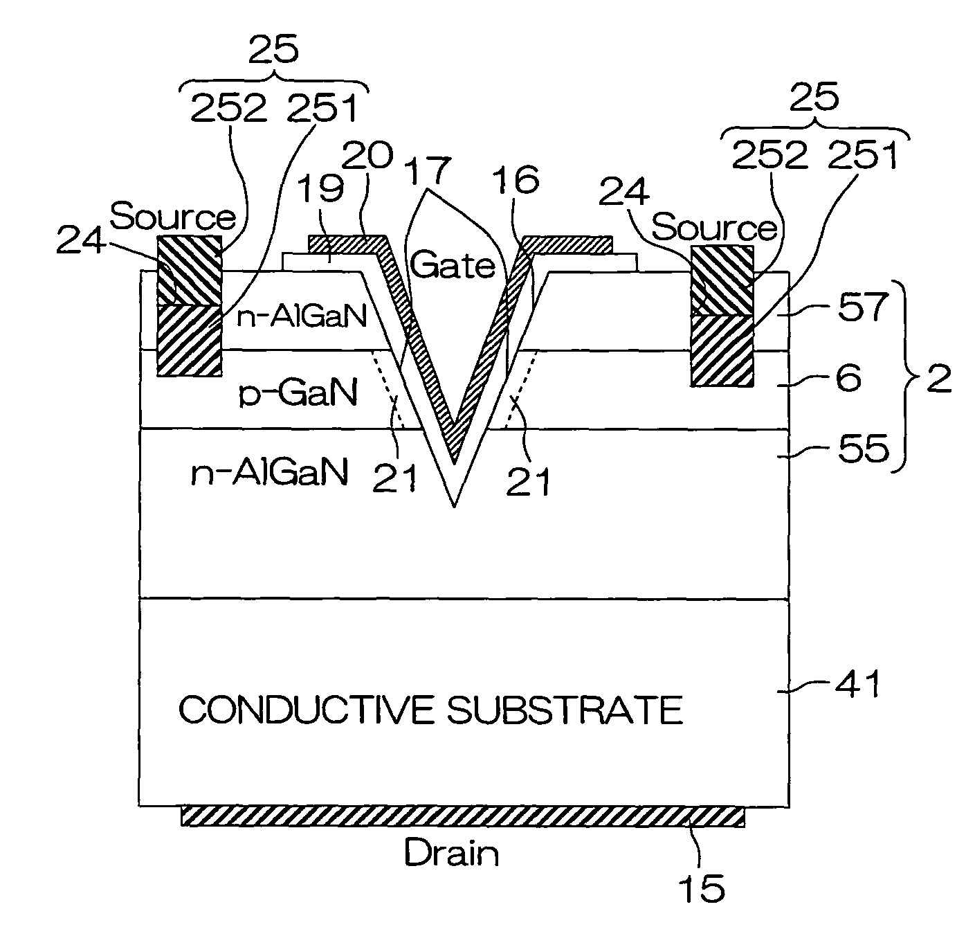
[0112]FIG. 4 is a schematic sectional view for illustrating the structure of an MIS field-effect transistor according to the present invention. Referring to FIG. 4, reference numerals identical to those in the case of FIG. 1 are allocated to portions corresponding to the portions in the above FIG. 1.

[0113]According to this embodiment, a conductive substrate 41 is employed. A nitride semiconductor multilayer structure portion 2 is formed on one surface of this conductive substrate 41. According to this embodiment, the nitride semiconductor multilayer structure portion 2 is constituted of an N-type GaN layer 5 formed on the surface of the conductive substrate 41, a P-type GaN layer 6 stacked thereon, and an N-type GaN layer 7 stacked thereon. A drain electrode 15 is formed in contact with the other surface of the conductive substrate 41. In this embodiment, therefore, it follows that the drain electrode 15 is electrically connected to the N-type GaN layer 5 through the conductive subs...

third embodiment

[0122]FIG. 6 is a schematic sectional view for illustrating the structure of an MIS field-effect transistor according to the present invention. Referring to FIG. 6, the same reference numerals are allocated to portions corresponding to the respective portions shown in the above FIG. 4. According to this embodiment, no substrate is provided, while a drain electrode 15 is formed in contact with a surface opposite to a gate electrode 20 in a nitride semiconductor multilayer structure portion 2. More specifically, the drain electrode 15 is applied / formed to generally cover the overall region of the lower surface (surface opposite to the gate electrode 20) of an N-type GaN layer 5. Therefore, this field-effect transistor can be formed in an extremely small thickness, and the thickness of the overall device reaching the upper surface(s) of the gate electrode 20 or source electrodes 25 from the drain electrode 15 can be set to not more than 30 μm. Further, electrons flowing into the N-type...


PUM

PropertyMeasurementUnit
thicknessaaaaaaaaaa
conductivity typeaaaaaaaaaa
conductivityaaaaaaaaaa

Abstract

The semiconductor device includes a P-type group III-V nitride semiconductor layer, an N-type group III-V nitride semiconductor layer, and an electrode in contact with both of the P-type group III-V nitride semiconductor layer and the N-type group III-V nitride semiconductor layer. The electrode includes a first electrode portion made of a first conductive material, and a second electrode portion, made of a second conductive material different from the first conductive material, bonded to the first electrode portion. The first electrode portion is in contact with the P-type group III-V nitride semiconductor layer, and the second electrode portion is in contact with the N-type group III-V nitride semiconductor layer.

Description

TECHNICAL FIELD[0001]The present invention relates to a semiconductor device (particularly an MIS field-effect transistor) employing group III-V nitride semiconductors and a method for manufacturing the same.PRIOR ART[0002]In general, a power device employing a silicon semiconductor is employed for a power amplifier circuit, a power supply circuit, a motor driving circuit or the like.[0003]However, improvement in breakdown voltage, reduction in resistance and improvement in speed of a silicon device are now reaching limits due to the theoretical limit of the silicon semiconductor, and it is becoming difficult to satisfy requirements of the market.[0004]Therefore, development of a GaN device having characteristics such as a high breakdown voltage, a high-temperature operation, a high current density, high-speed switching and small on-resistance is examined (following Non-Patent Document 1).[0005]Patent Document 1: Japanese Unexamined Patent Publication No. 2004-260140[0006]Patent Doc...

Claims


Application Information

Patent Timeline
Patent Type & Authority Patents(United States)
IPC IPC(8): H01L31/0328
CPCH01L29/205H01L29/66462H01L29/66666H01L29/66734H01L29/7786H01L29/7813H01L29/7827H01L29/802H01L29/0873H01L29/0878H01L29/2003H01L29/41766H01L29/4236H01L29/432H01L29/456
Inventor OHTA, HIROAKITAKASU, HIDEMI
Owner ROHM CO LTD
Why Eureka
Try Eureka