
Method and apparatus for positioning and contacting singulated semiconductor dies

Inactive Publication Date: 2011-10-25
BURGYAN LAJOS
View PDF12 Cites 38 Cited by
  • Summary
  • Abstract
  • Description
  • Claims
  • Application Information

AI Technical Summary

Benefits of technology

[0025]The architecture of miniaturized of the re-useable macro scale test socket components that reduce parasitic electrical and magnetic field effects including inductances, capacitances and resistances in conduction through-paths provided by the test socket; and
[0032]A primary advantage of the described test socket stems from a compact macro alignment and latch mechanisms allowing for very small test sockets, having much reduced parasitic inductive, capacitive and resistive affects, that occupies a very small space on the PCB, thus even further reducing the magnitude of resistive and other of undesirable electrical and magnetic field effects that can color the parameters of the DUT being analyzed.

Problems solved by technology

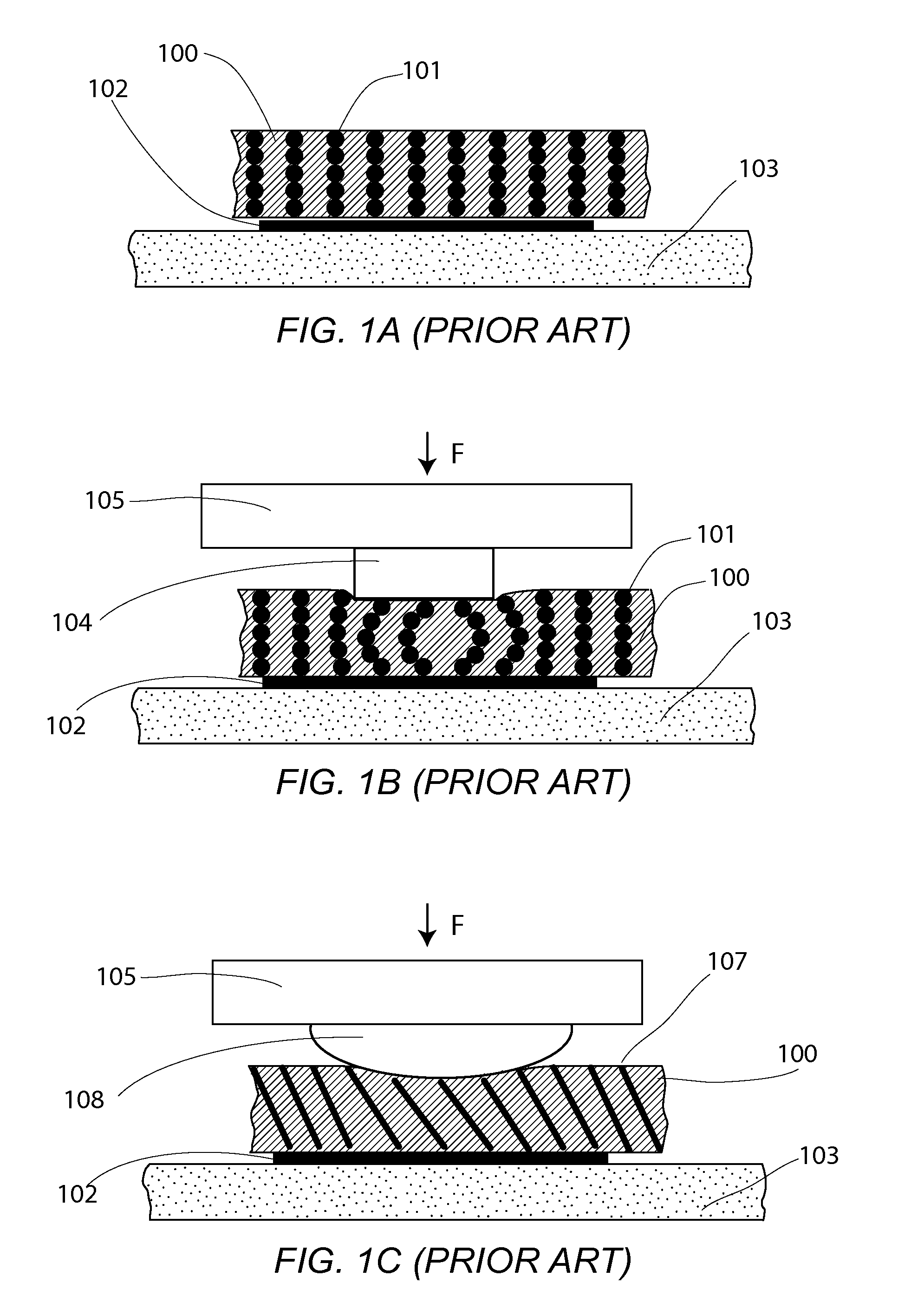
Such systems are typically limited by the particular architecture of the actual test socket that connects between terminals of such integrated circuit packages and the test equipment in final testing stages of design, development, prototyping and manufacturing of integrated circuit packages being tested or examined and are commonly referred to by an acronym DUT, meaning ‘Device Under Test’.
While such critical components can often be placed on the opposite (bottom) side of the testing printed circuit board (PCB), parasitic inductance of such conductive paths through the PCB often can interfere with proper operation of the DUT.
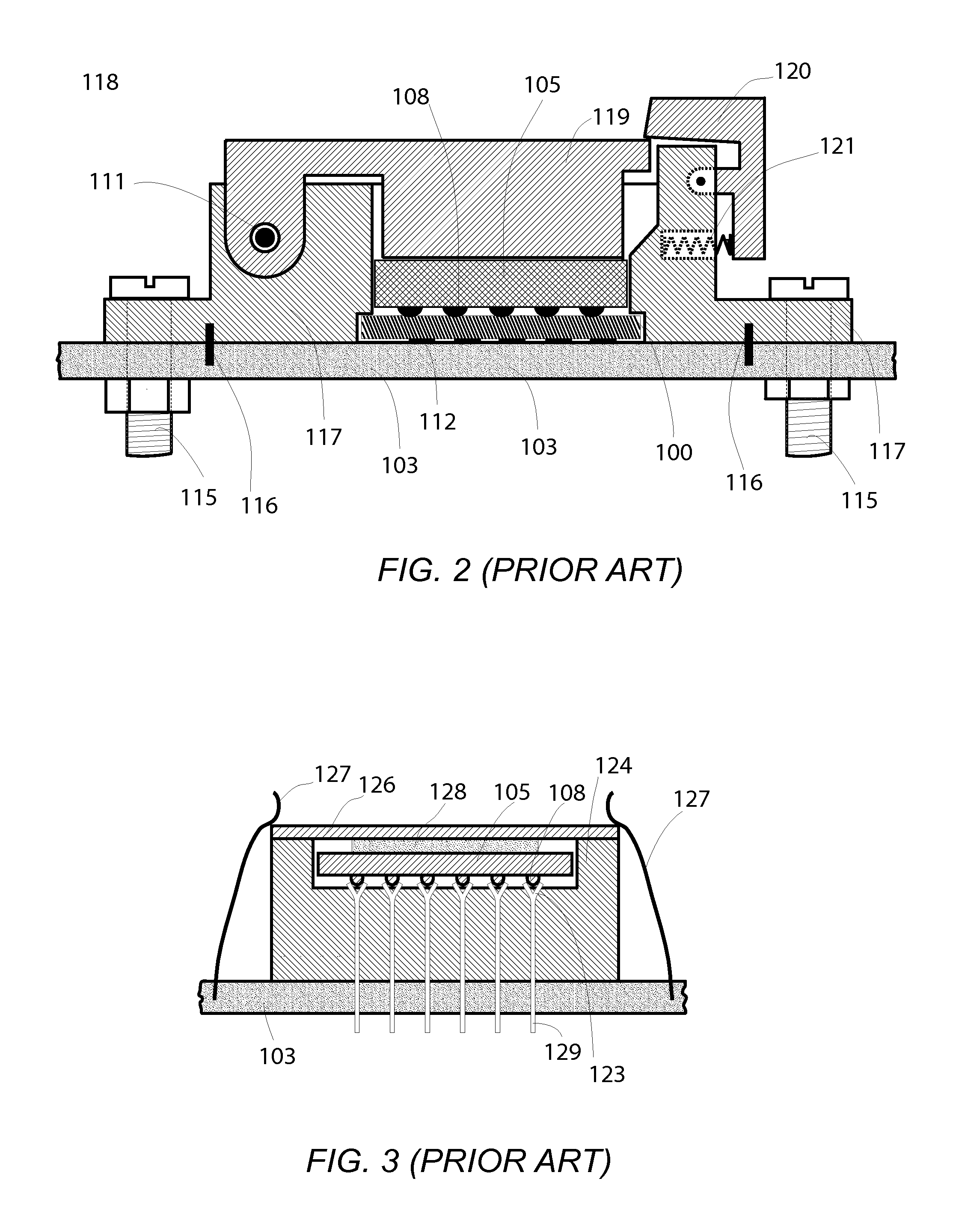
Also, the complex mechanical designs of typical prior art test sockets (FIG. 2) present a number of fabrication challenges.
Fabrication is labor intensive, and high mechanical precision must be maintained, while using conventional mechanical machine shop fabrication techniques and extensive tooling changes.
Economically, fabrication costs of such prior art test socket systems typically require minimum quantity orders in multiple thousands of dollars range.
Another problem with test socket system like those of FIG. 3 is the apparent lack of compliance range.
Other problems with prior art test socket systems and test socket architectures relate to the increasing complexity and number of input / output connectors of current and evolving integrated circuit packages.
In the past, test socket manufacturers have relied upon conventional mechanical engineering and associated expensive labor intensive, above-and-beyond machine shop techniques to meet the ever-increasing demand for complex testing system and appropriate architecture for test sockets.
Versatile, re-configurable test sockets for testing a wide variety of IC / semiconductor packages [DUT] of different sizes, and terminal styles having re-useable elements are currently unavailable from the test socket industry.

Method used


Image

  • Method and apparatus for positioning and contacting singulated semiconductor dies
  • Method and apparatus for positioning and contacting singulated semiconductor dies
  • Method and apparatus for positioning and contacting singulated semiconductor dies

Examples


Embodiment Construction

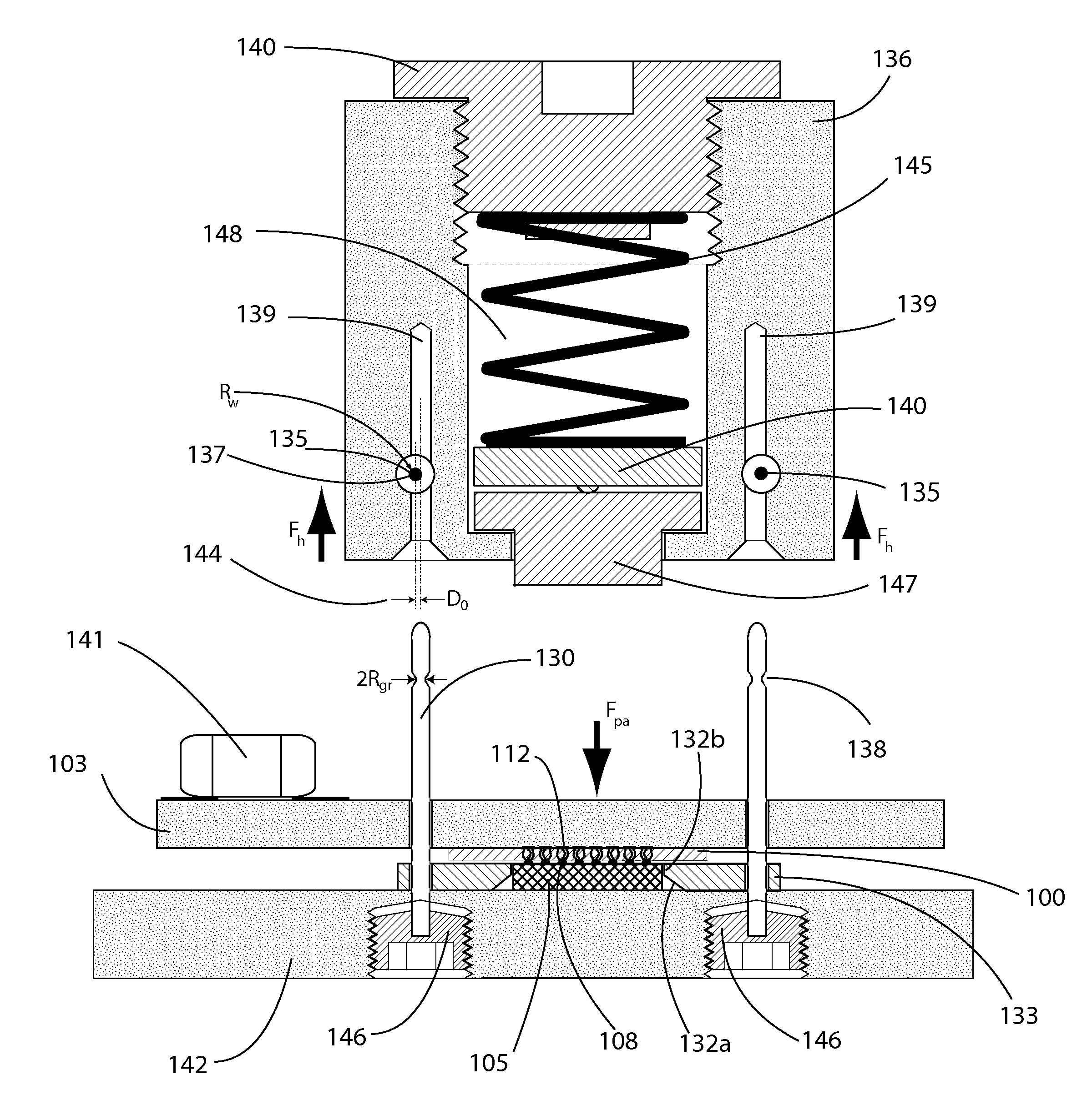
[0048]Features of preferred embodiments the invented test socket and related methods and processes for achieving the advantages and performance improvements of the invented test socket system and architecture are described herein with reference to the accompanying drawings. However, known mechanical and related electrical systems associated with testing systems for semiconductor IC DUT packages are not described in detail.

[0049]FIG. 4 shows an exploded, perspective view of the architectural components of the invented test socket 150 system for positioning a DUT package 105 having particular perimeter dimensions presenting a planar bottom surface, microarray of electrically conductive connectors 108 for testing on a flat surface of a test PCB 103 presenting a corresponding top surface, planar microarray of electrically conductive connector traces 112 (not shown, see FIGS. 2, 5&7a).

[0050]In more detail, with reference to FIG. 4, the functionality and advantages afforded by the invente...


PUM


Abstract

A re-configurable test socket system and test socket architecture are described involving a combination of particular micro elements and re-useable macro elements that can be reused and reconfigured for testing a wide variety of different semiconductor and integrated circuit (IC) DUT packages having different shapes, sizes, and terminal configurations.

Description

RELATED APPLICATIONS[0001]This Application claims all benefits applicable under 35 U.S.C. §119(e) related to U.S. Provisional Patent Application Ser. No. 61 / 329,087 filed by the Applicant on 28 Apr. 2010 entitled “METHOD AND APPARATUS FOR POSITIONING AND CONTACTING SINGULATED BUMPED SEMICONDUCTOR DIES AND QFN DEVICES”, and incorporates U.S. Provisional Patent Application Ser. No. 61 / 120,822, in its entirety, by reference into this application.FIELD OF THE INVENTION[0002]The present invention relates generally to test sockets for evaluating performance of an integrated circuit (ICs) or semiconductor device. More particularly, the present invention relates to a test sockets system and manufacture of particular test socket architecture developed for testing micron dimensioned integrated circuits (IC / semiconductor chip packages) having solder pad, solder ball, copper pillar or similar type terminals.BACKGROUND OF THE INVENTION[0003]Test socket systems are essential and widely used in de...

Claims


Application Information

Patent Timeline
IPC IPC(8): G01R31/00G01R31/20G01R31/02
CPCG01R1/0466G01R1/0483
Inventor BURGYAN, LAJOS
Owner BURGYAN LAJOS
Learn More