Atomic layer removal process with higher etch amount

a technology of atomic layer and etching amount, which is applied in the direction of basic electric elements, semiconductor/solid-state device manufacturing, electric apparatus, etc., can solve the problems of increasing the effectiveness of “reset”, limiting the amount of material that may be etched per cycle, and increasing the total process time. , to achieve the effect of improving the overall etch rate and throughput of the alr etch process, excellent process control, and limiting the amount of material

Inactive Publication Date: 2011-11-15
NOVELLUS SYSTEMS
View PDF63 Cites 301 Cited by
  • Summary
  • Abstract
  • Description
  • Claims
  • Application Information

AI Technical Summary

Benefits of technology

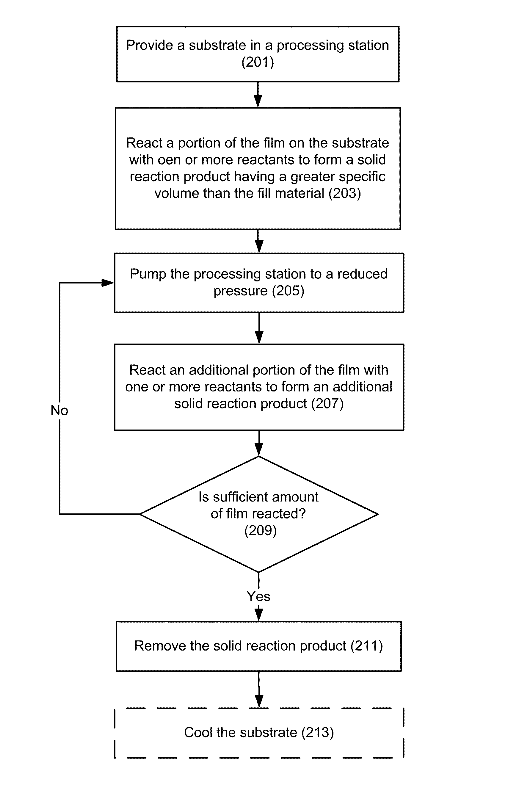
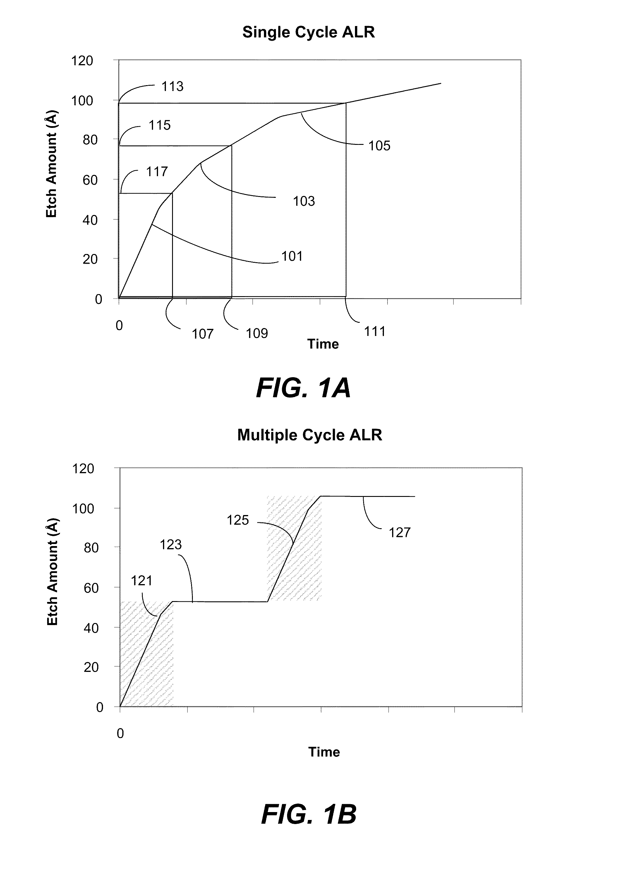
[0005]Atomic layer removal (ALR) etch is a process that offers excellent process control. In ALR, a film material is reacted to form a solid reaction product having a greater specific volume than the film material it consumes. The solid reaction product is sublimated and removed. The reaction is self-saturating, thus limiting the amount of material that may be etched per cycle. Multiple cycl

Problems solved by technology

The reaction is self-saturating, thus limiting the amount of material that may be etched per cycle.
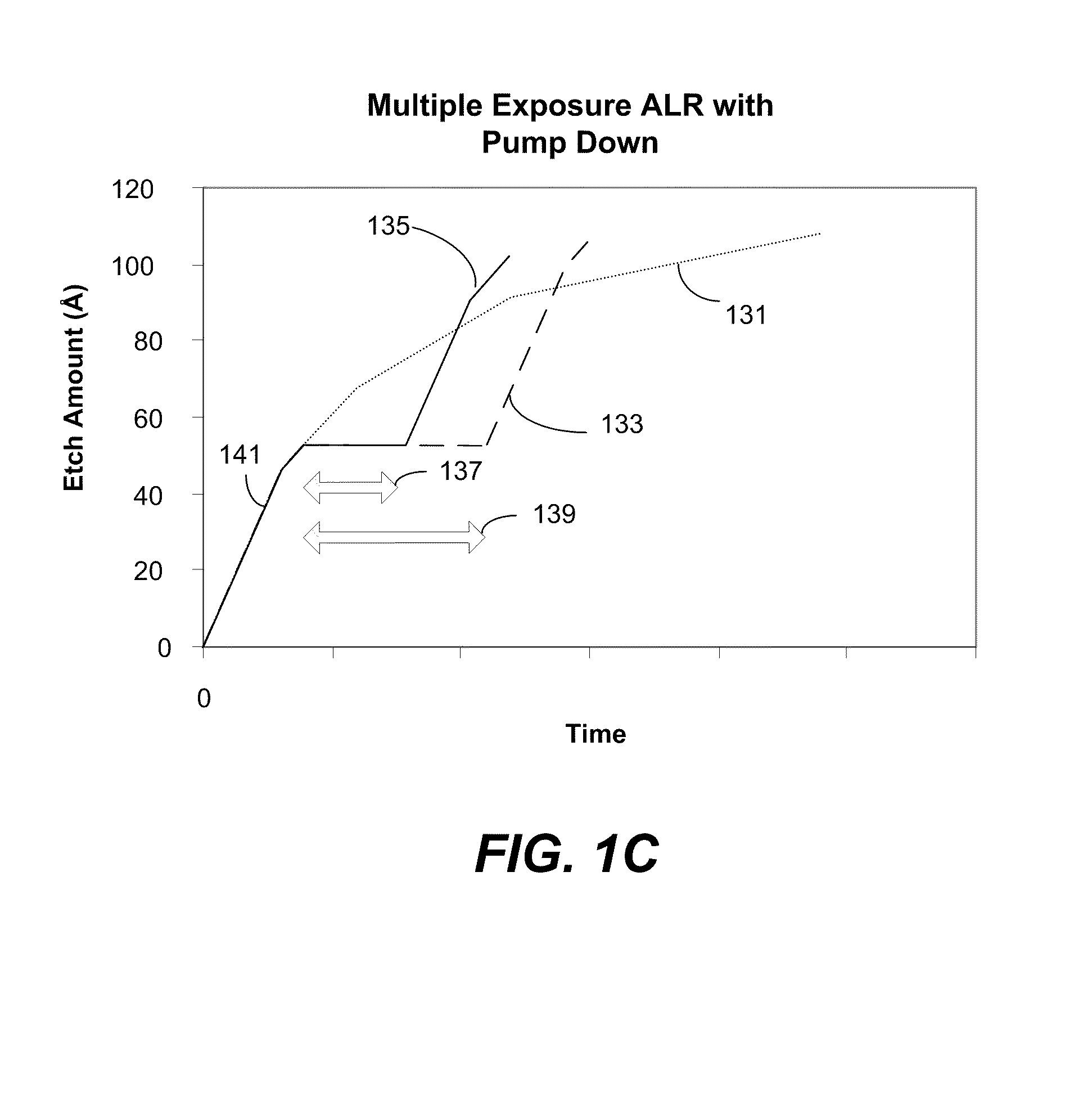
However, the increase in effectiveness of the “reset” is off

Method used


Image

  • Atomic layer removal process with higher etch amount
  • Atomic layer removal process with higher etch amount
  • Atomic layer removal process with higher etch amount

Examples


Embodiment Construction

Introduction

[0024]Embodiments of the present invention are described herein in the context of etching a substrate with blanket dielectric film and the context of filling a gap with dielectric material. Those of ordinary skill in the art will realize that the following detailed description of the present invention is illustrative only and is not intended to be in any way limiting. Other embodiments of the present invention will readily suggest themselves to such skilled persons having the benefit of this disclosure. For example, the gap fill application may be for shallow trench isolation (STI), inter-layer dielectric (ILD), inter-metal dielectric (IMD), or pre-metal dielectric (PMD).

[0025]Reference will be made in detail to implementations of the present invention as illustrated in the accompanying drawings. The same reference indicators will be used throughout the drawings and the following detailed description to refer to the same or like parts. In this application, the terms “wor...


PUM

PropertyMeasurementUnit
Temperatureaaaaaaaaaa
Partial pressureaaaaaaaaaa

Abstract

Higher overall etch rate and throughput for atomic layer removal (ALR) is achieved. The reaction is a self-limiting process, thus limiting the total amount of material that may be etched per cycle. By pumping down the process station between reacting operations, the reaction is partially “reset.” A higher overall etch rate is achieved by a multiple exposure with pump down ALR process.

Description

FIELD OF THE INVENTION[0001]This invention relates to electronic device fabrication processes and associated apparatus. More specifically, it relates to dry etch processes for removing dielectric films.BACKGROUND OF THE INVENTION[0002]It is often necessary in semiconductor processing to remove or etch dielectric films from a substrate surface. Various etching processes are available to etch different materials and geometries at different rates. Considerations for choosing the appropriate etch process include etch rates, selectivity to other materials, by-products, and ability to finely control the process. Regarding etch rates, rates for the material to be removed and rates for the material to remain at various geometries may be considered. Some etch processes are isotropic, etching evenly at all surfaces. Others are anisotropic. A higher etch rate is usually preferred, accompanied by a lower etch rate for the material intended to remain. This etch selectivity may be based on materi...

Claims


Application Information

Patent Timeline
IPC IPC(8): H01L21/302
CPCH01L21/02164H01L21/02274H01L21/02337H01L21/31116H01L21/76837H01L21/02271
Inventor DRAEGER, NERISSATE NIJENHUIS, HARALDMEINHOLD, HENNERVAN SCHRAVENDIJK, BARTNITTALA, LAKSHMI
Owner NOVELLUS SYSTEMS
Why Eureka
Try Eureka