Oxynitride bilayer formed using a precursor inducing a high charge trap density in a top layer of the bilayer

a technology of oxynitride and a top layer, applied in the field of oxidenitrideoxide (ono) stack or structure including an oxynitride bilayer, can solve the problems of limiting the device b>100/b> lifetime and/or its use in several applications, and reducing the efficiency of b>206/b>, and achieves only moderate improvemen

Active Publication Date: 2011-11-29
LONGITUDE FLASH MEMORY SOLUTIONS LTD
View PDF19 Cites 34 Cited by
  • Summary
  • Abstract
  • Description
  • Claims
  • Application Information

AI Technical Summary

Benefits of technology

[0014]In another aspect, the present invention is directed to a semiconductor device including a bilayer charge storing layer comprising a first layer including a substantially trap free oxynitride layer, and a second layer formed on a surface of the first layer including an oxynitride charge trapping laye

Problems solved by technology

One problem with conventional ONO and SONOS structures 102 and methods of forming the same is the single, homogenous nitride or oxynitride layer 118 that is used as a charge retention or memory layer, and which can have poor or decreasing data retention over time, limiting the device 100 lifetime and/or its use in several applications due to leakage current through the layer.
Moreover, the slope of Vt in retention mode is still appreciably steep and the leakage path is not sufficiently minimized to significantly improve data retention, thus EOL 206 is only moderately improved.
Anoth

Method used


Image

  • Oxynitride bilayer formed using a precursor inducing a high charge trap density in a top layer of the bilayer
  • Oxynitride bilayer formed using a precursor inducing a high charge trap density in a top layer of the bilayer
  • Oxynitride bilayer formed using a precursor inducing a high charge trap density in a top layer of the bilayer

Examples


Embodiment Construction

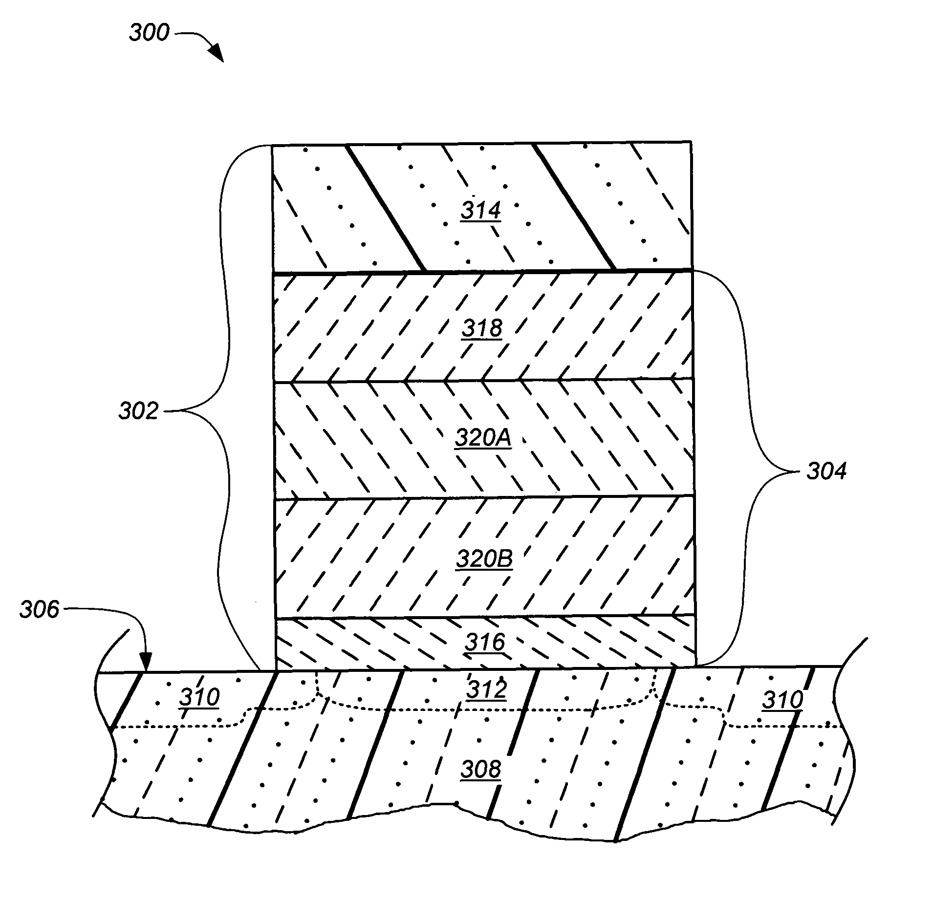
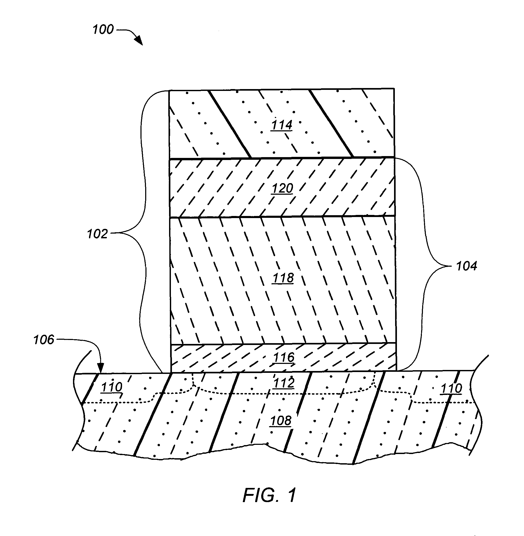
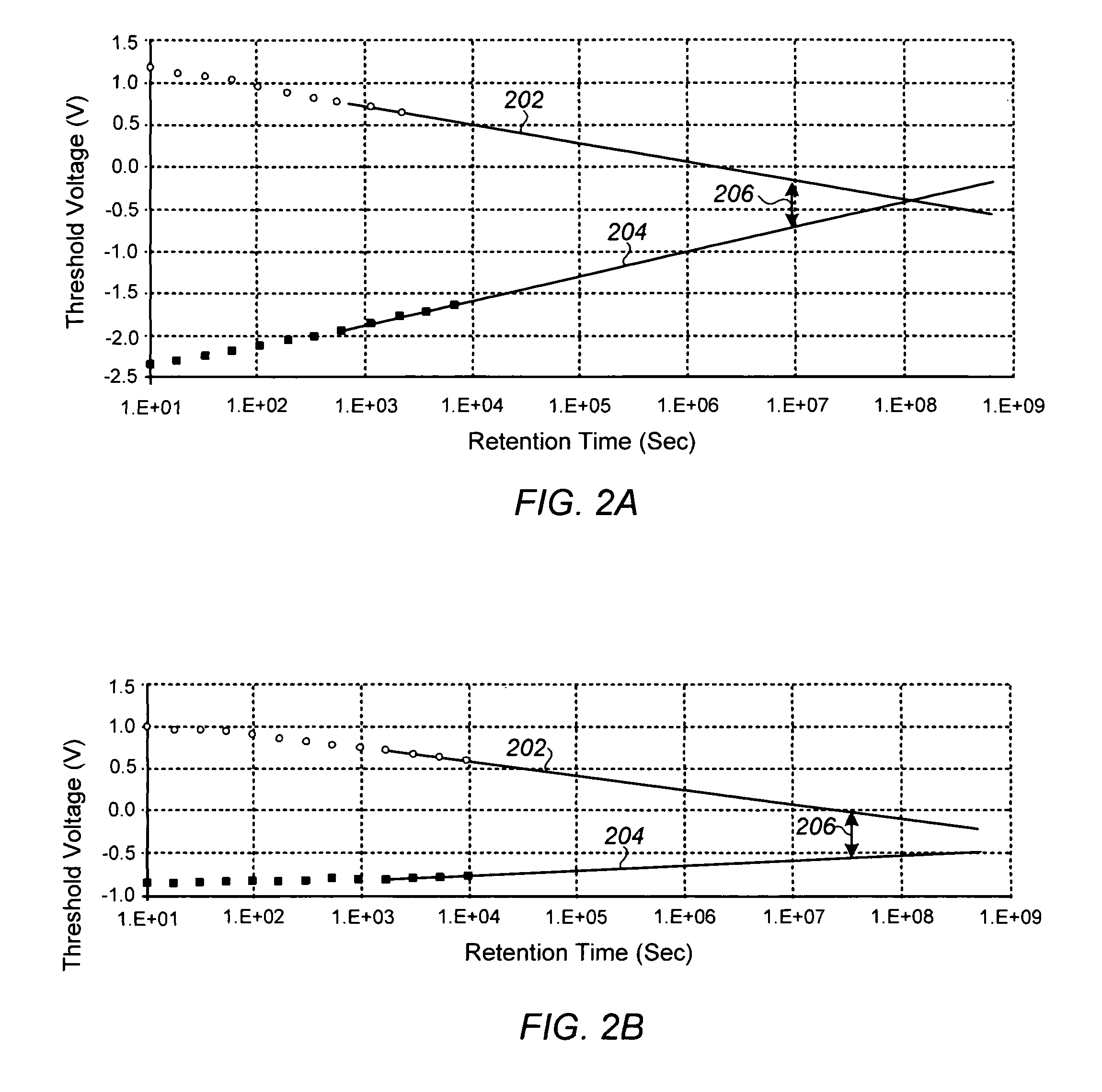
[0022]The present invention is directed generally to an oxide-nitride-oxide (ONO) structure including an oxynitride bilayer as a charge storing layer and methods for making the same. The ONO structure and method are particularly useful for forming a memory layer in a memory device, such as a silicon-oxide-nitride-oxide-silicon (SONOS) memory transistor.

[0023]In the following description, for purposes of explanation, numerous specific details are set forth in order to provide a thorough understanding of the present invention. It will be evident, however, to one skilled in the art that the present invention may be practiced without these specific details. In other instances, well-known structures, and techniques are not shown in detail or are shown in block diagram form in order to avoid unnecessarily obscuring an understanding of this description.

[0024]Reference in the description to “one embodiment” or “an embodiment” means that a particular feature, structure, or characteristic des...


PUM


Abstract

A semiconductor device including a bilayer charge storing layer and methods of forming the same are provided. Generally, the method includes: (i) forming a first layer of the bilayer charge storing layer; and (ii) forming a second layer formed on a surface of the first layer, the second layer including an oxynitride charge trapping layer. Preferably, the first layer includes a substantially trap free oxynitride layer. More preferably, the oxynitride charge trapping layer includes a significantly higher stoichiometric composition of silicon than that of the first layer. In certain embodiments, the oxynitride charge trapping layer has a concentration of carbon selected to increase the number of traps therein. Other embodiments are also disclosed.

Description

CROSS-REFERENCE TO RELATED APPLICATIONS[0001]The present application claims the benefit of priority under 35 U.S.C. 119(e) to U.S. Provisional Patent Application Ser. No. 60 / 931,948 entitled “SONOS Stack With Oxynitride Bilayer Made Of BTBAS And NH3,” filed May 25, 2007, which application is hereby incorporated by reference in its entirety.TECHNICAL FIELD[0002]This invention relates to semiconductor processing and, more particularly to an oxide-nitride-oxide (ONO) stack or structure including an oxynitride bilayer that exhibits improved charge storing for data retention and to methods of forming the same.BACKGROUND OF THE INVENTION[0003]Non-volatile semiconductor memories, such as a split gate flash memory, typically use a stacked floating gate type field effect transistors, in which electrons are induced into a floating gate of a memory cell to be programmed by biasing a control gate and grounding a body region of a substrate on which the memory cell is formed.[0004]In particular, ...

Claims


Application Information

Patent Timeline
IPC IPC(8): H01L21/336
CPCH01L21/0214H01L21/022H01L21/02211H01L21/02219H01L21/02222H01L21/02271H01L21/28282H01L29/513H01L29/792H01L29/40117
Inventor LEVY, SAGY
Owner LONGITUDE FLASH MEMORY SOLUTIONS LTD
Why Eureka
Try Eureka