Transformer

a transformer and transformer technology, applied in the field of transformers, can solve problems such as deterioration of gain or tolerable coupling noise characteristics, and achieve the effect of accurate formation

Active Publication Date: 2011-12-06
DENSO CORP
View PDF10 Cites 11 Cited by
  • Summary
  • Abstract
  • Description
  • Claims
  • Application Information

AI Technical Summary

Benefits of technology

[0005]When a semiconductor layer formed on a semiconductor substrate is used as a first coil as in the case of Japanese Patent Application Publication No. H07-183468, an insulating layer conventionally formed between a silicon substrate and the first coil can be eliminated, and the microtransformer can be downsized thereby. On the other hand, a semiconductor layer has a higher series resistance than a metal layer. Therefore, simply replacing the first coil composed of a metal layer with the first coil composed of the semiconductor layer results in deterioration of a gain or a tolerable coupling noise characteristic of the microtransformer.
[0006]An object of the present teachings is to provide a transformer capable of achieving both downsizing and property retention of a microtransformer.
[0008]With this transformer, a first coil is constituted by the semiconductor layer coil and the trench coil connected with each other in parallel on the surface of the first conductivity type semiconductor layer and a second coil is constituted by the metal layer coil. Since the semiconductor layer coil of the first coil uses the semiconductor layer as the coil wiring, an insulating layer between the first conductivity type semiconductor layer and the first coil can be eliminated and the microtransformer can be downsized. In addition, since the trench coil and the semiconductor layer coil are connected with each other in parallel, a resistance of the first coil can be reduced. Further, the semiconductor layer coil wiring and the trench coil wiring respectively have spiral shapes and are alternately disposed in the radial direction thereof. As a result, properties of the microtransformer such as gain and tolerable coupling noise can be retained.
[0010]A method for manufacturing the transformer described above preferably includes the steps of forming the trench coil in the first conductivity type semiconductor layer; and forming the semiconductor layer coil by performing ion injection to the first conductivity type semiconductor layer between trench coil wiring of the trench coil formed in the previous step. According to such a manufacturing method, a semiconductor layer coil can be accurately formed.

Problems solved by technology

Therefore, simply replacing the first coil composed of a metal layer with the first coil composed of the semiconductor layer results in deterioration of a gain or a tolerable coupling noise characteristic of the microtransformer.

Method used


Image

  • Transformer
  • Transformer
  • Transformer

Examples


Embodiment Construction

[0017]Hereinafter, a first embodiment of the present teachings will be described with reference to the drawings. In the embodiment, a transformer whose first conductivity type is the p-type and whose second conductivity type is the n-type will be exemplified and described.

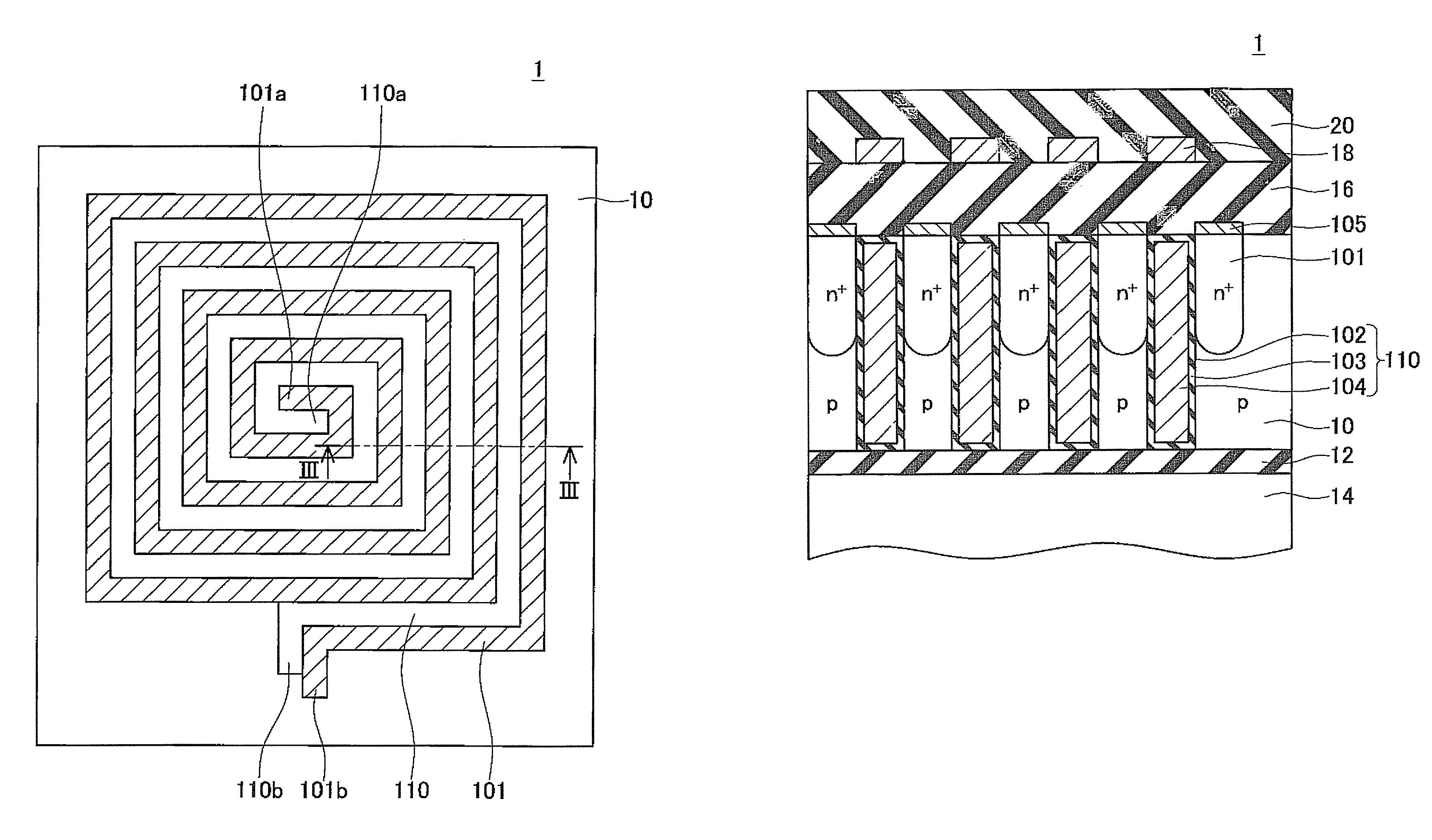
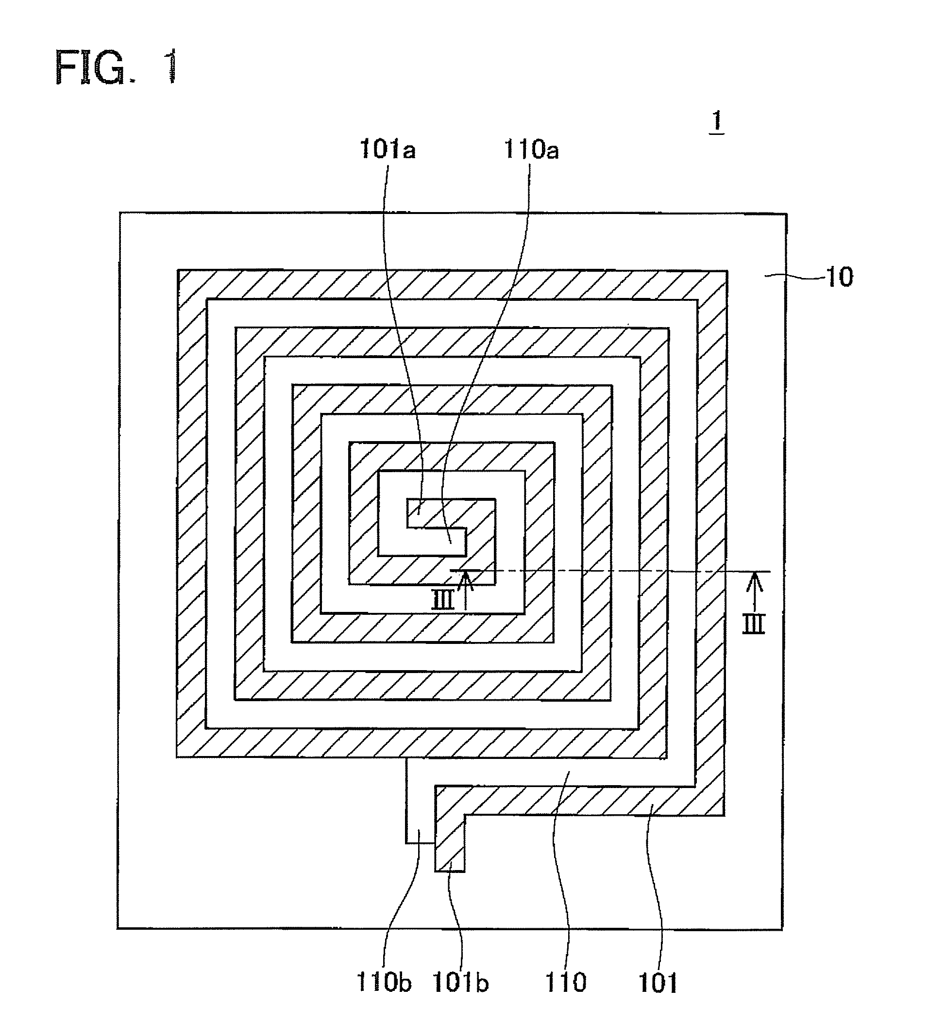
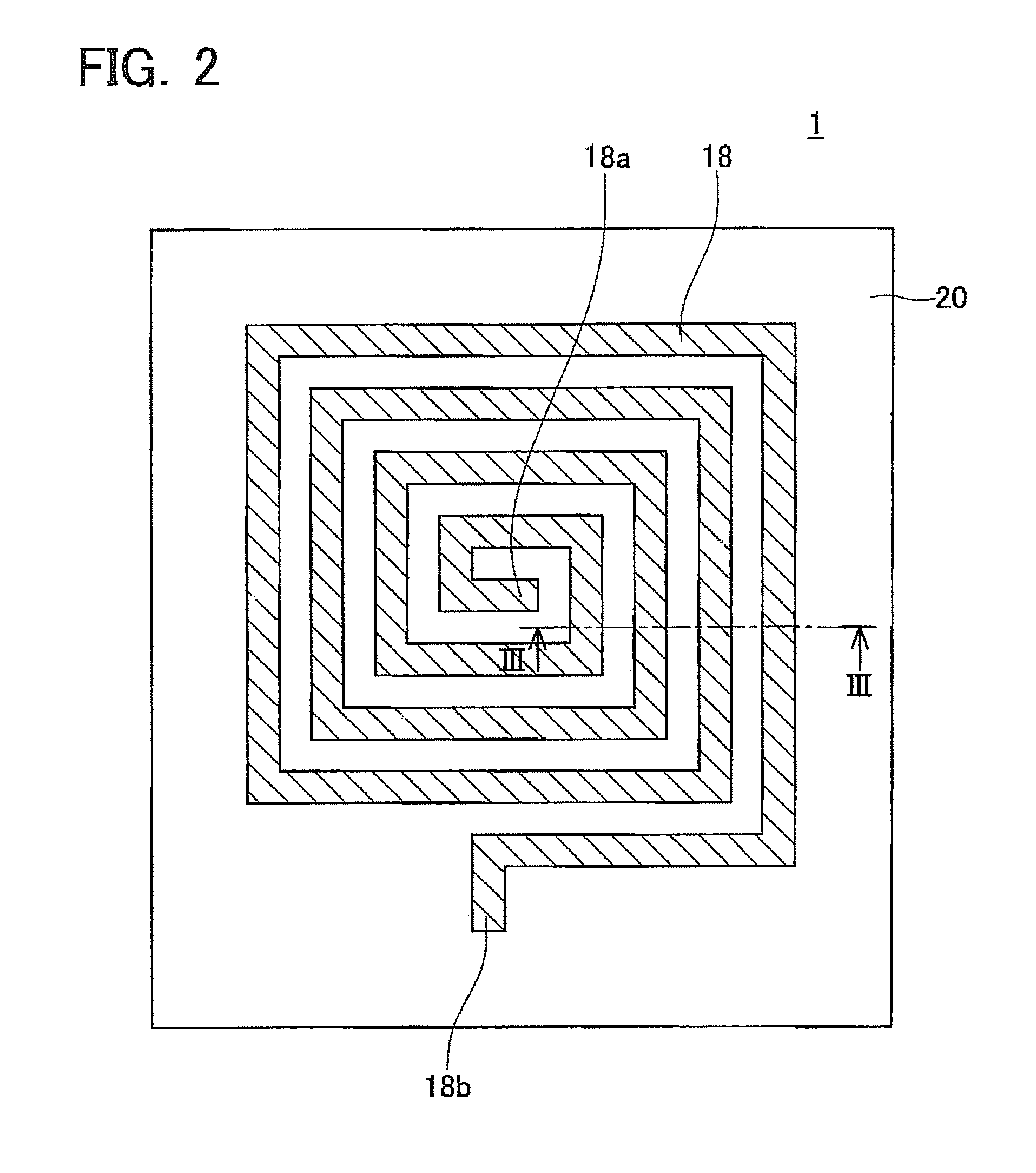
[0018]FIGS. 1 and 2 are diagrams illustrating a microtransformer according to the embodiment. FIG. 1 illustrates a plan view of a microtransformer 1 sectioned along a plane including the first coil, and FIG. 2 illustrates a plan view of the microtransformer 1 sectioned along a plane including the second coil. FIG. 3 is a cross-sectional view of the microtransformer 1 illustrated in FIGS. 1 and 2 taken along line III-III. FIG. 4 is a conceptual diagram illustrating a transmitter / receiver comprising the microtransformer 1, a transmitter circuit 3, and a receiver circuit 5.

[0019]As illustrated in FIGS. 1 to 3, the microtransformer 1 comprises a lower substrate 14, an insulating layer 12 making contact with a surface o...


PUM

PropertyMeasurementUnit
conductivityaaaaaaaaaa
conductiveaaaaaaaaaa
metallicaaaaaaaaaa

Abstract

A transformer may include a semiconductor layer coil, a trench coil connected with the semiconductor layer coil in parallel, and a metal layer coil opposing both of the semiconductor layer coil and the trench coil. The semiconductor layer coil and the trench coil may be insulated from the metal layer coil by an insulating layer.

Description

CROSS-REFERENCE TO RELATED APPLICATION[0001]This application claims priority to Japanese Patent Application No. 2009-269875 filed on Nov. 27, 2009, the contents of which are hereby incorporated by reference into the present application.TECHNICAL FIELD[0002]The present teachings relate to a transformer that performs signal transmission between electrically-insulated electrical circuits.DESCRIPTION OF RELATED ART[0003]There are methods of performing signal transmission between electrically-insulated electrical circuits so as to prevent an excessive current from flowing when a high voltage is suddenly applied such as during a surge. One such method utilizes inductive coupling by a transformer. Due to ongoing downsizing, transformers are now small enough to be integrated with integrated circuits. Hereinafter, such a small transformer shall be referred to as a microtransformer.[0004]Conventionally, a microtransformer formed by laminating, on a silicon substrate surface, an insulating lay...

Claims


Application Information

Patent Timeline
Patent Type & Authority Patents(United States)
IPC IPC(8): H01F5/00H01F27/28H01L27/08
CPCH01F27/2804H01L23/645H01L2924/14H01L2924/19042H01L2924/30105H01L2224/48091H01L2924/30107H01L2924/00014
Inventor KIJIMA, SHINYA
Owner DENSO CORP
Why Eureka
Try Eureka